Name
Ref.
Desg.
J1
Description
+B
This is the positive supply pin usually connected to +12VDC.
RXIN
TXIN
J2
J3
This is the input to the audio band pass filter in RX mode.
This is the TX Audio Input pin. In the TX mode it may be pre-filtered, using the
TX audio path, Thus helping to avoid talkoff due to intermodulation of low
frequency speech components with the transmitted CTCSS tone.
This is the band pass filtered transmit audio output pin. In TX mode the pin
outputs audio present at the TX audio input pin.
In RX mode this pin operates as a "Push To Listen" function by enabling the RX
audio path, thus overriding the tone squelch function. Tying PTL to ground will
inhibite audio through the RX audio path till a CTCSS tone is decoded or “No
Tone” is selected on D0-D5
TXOUT
PTL
J4
J5
RXOUT
J6
This is the band pass filtered receive audio output pin. This pin outputs audio
when RX tone DECODE is true or PTL is true or when Notone is programmed.
Logic level input pulled low to enable transmitt mode.
J7
J8
PTT
TONEOUT
The CTCSS sine wave output appears on this pin under control of the PTT
input. The level is adjusted using R3.
CARRIER
SENSE
J9
Input that can be connected to the radios carrier sense logic to enable the
CTCSS decoder only when a carrier is present.
DECODE
J10
This is an open collector output used to mute the RX audio path or control
squelch circuitry in a system. It provides a path to ground when a CTCSS tone is
not present and is open collector when a CTCSS tone is detected.
This pin will have a +5VDC output till a CTCSS tone is detected. Alternatively
this pin can be used to disable the open collector DECODE output pin and can
J11
MONIT0R
+5V
be connected to a system’s "Push To Listen", or MONIT0R function.
J12
This pin is an alternative supply pin that can be connected to an external DC
supply to evaluate performance of the MX465 at supply voltages below 7.0 VDC.
Connection to ground.
In serial operation, Data to control the MX465 is clocked in on this logic input.
Refer to the MX465’s data sheet for operation.
GND
SERIAL DATA
J13
J14
SERIAL CLOCK
LOAD LATCH
J15
J16
Control data is clocked into the MX465 based on the rising and falling edge of
this logic input.
Data is either in the process of loading into the MX465 control registers or is
latched into the MX465’s internal registers using this logic input pin.
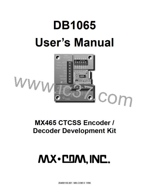
Table 2: Connector Signal Descriptions
Page 15
20480150.001 MX-COM ꢀ 1996

 CMLMICRO [ CML MICROCIRCUITS ]