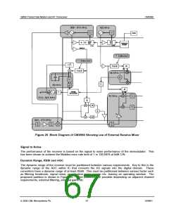
GMSK Packet Data Modem and RF Transceiver
CMX990
7.
Performance Specification
7.1
Electrical Performance
7.1.1 Absolute Maximum Ratings
Exceeding these maximum ratings can result in damage to the device.
Min.
Max.
4.0
3.0
Unit
V
V
Supply (VDDH - VSSH and VDDVCO - VSSH only)
-0.3
-0.3
-0.3
-100
-20
Supply (All other VDD - VSS
)
Voltage on any pin to VSSH
Current into or out of any VDD or VSS pin
Current into or out of any other pin
VDD + 0.3
+100
+20
V
mA
mA
V
Voltage between any 2 VSS pins
-0.3
-0.3
+0.3
+0.3
Voltage between any 2 VDD pins (except VDDH
)
V
Q1 Package
Total Allowable Power Dissipation at TAMB = 25 °C
... Derating above 70 °C
Storage Temperature
Operating Temperature
Min.
–
–
-55
-40
Max.
1000
26.5
+125
+85
Unit
mW
mW/°C
°C
°C
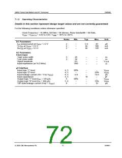
7.1.2 Operating Limits
Correct operation of the device outside these limits is not implied.
Notes
Min.
3.0
3.0
Max.
3.6
3.6
Units
Supply (VDDH - VSSH
Supply (VDDVCO - VSSH
Supply (All other VDD - VSSH
)
V
V
V
)
)
2.25
2.75
Voltage difference between supplies:
VDDH to VDDVCO
Between all other VDD
All VSS to VSSH
Operating Temperature
Clock Frequency
0
0
0
-40
3.8
±0.2
±0.2
±50
+85
24
V
V
mV
°C
1
MHz
Notes:
1
Error in RF and IF frequencies and bit rate is directly related to the clock frequency.
ã 2004 CML Microsystems Plc
71
D/990/1

 CMLMICRO [ CML MICROCIRCUITS ]