GMSK Packet Data Modem and RF Transceiver
CMX990
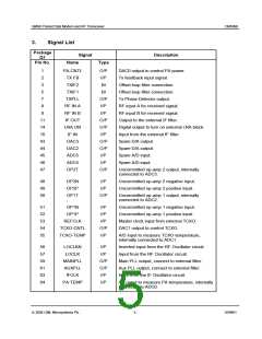
Package
Signal
Q1
Description
Pin No.
Name
Type
4
VDD Tx
VSS Tx
Power
Power
Power
Power
Power
Power
Power
Power
O/P
Power supply to Tx IF and RF circuits.
Return for VDD Tx, good decoupling required.
Power supply to Rx RF circuits.
6
10
12
13
15
23
24
25
VDD Rx1
VSS Rx1
VSS Rx2
VDD Rx2
VDD Dig
VDD Ana
VBIAS
Return for VDD Rx1, good decoupling required.
Return for VDD Rx2, good decoupling required.
Power supply to Rx IF circuits.
Power supply to base band digital circuits.
Power supply to aux ADC, DAC, OP1/2 circuits.
Output of internal bias generator, decouple to
VSS Ana.
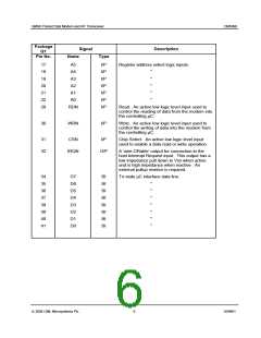
26
27
28
33
VSS Ana
VSS Dig
Power
Power
Power
Power
Return for VDD Ana, good decoupling required.
Return for VDD Dig, good decoupling required.
Return for VDD H, good decoupling required.
VSS
VDD
H
H
Power supply to host interface and 2.5V
regulator circuit.
42
58
60
V-CONT
VSS Synth
VDD VCO
O/P
Control signal for external regulating transistor.
Return for VDD Synth, good decoupling required.
Power
Power
Power supply to the VCO charge pump,
decouple to VSS H.
62
VDD Synth
Power
Power supply to synthesiser circuits.
Notes: I/P
=
=
=
=
=
Input
Output
Bidirectional
3-state Output
No Connection
O/P
BI
T/S
NC
ã 2004 CML Microsystems Plc
7
D/990/1

 CMLMICRO [ CML MICROCIRCUITS ]