GMSK Packet Data Modem and RF Transceiver
CMX990
CONTENTS
Section
Page
1.
2.
3.
4.
Brief Description..................................................................................1
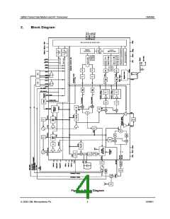
Block Diagram .....................................................................................4
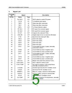
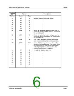
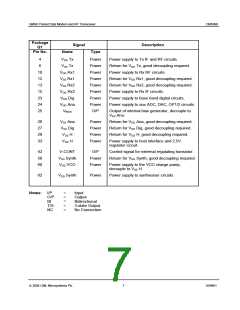
Signal List............................................................................................5
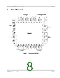
External Components..........................................................................8
4.1
4.2
4.3
4.4
4.5
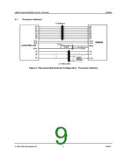
Processor Interface.................................................................9
Synthesiser and TCXO .........................................................10
Transmit ................................................................................11
Receive ..................................................................................12
Power Supply Decoupling and Layout ................................13
5
General Description...........................................................................15
5.1
Baseband Modem .................................................................15
5.1.1 Description of Blocks...............................................15
5.1.2 Modem - µC Interaction............................................17
5.1.3 Data Formats.............................................................18
5.1.4 Programmer’s View of the Modem ..........................20
5.1.5 CRC, FEC, Interleaving and Scrambling Details.....37
5.1.6 Application Notes.....................................................40
µC Interface ...........................................................................44
5.2.1 Memory Map and Interface.......................................44
5.2.2 Power-on and Reset .................................................45
5.2.3 Clock Control............................................................46
5.2.4 Status Registers .......................................................47
5.2.5 Write Only Registers ................................................48
5.2.6 Read Only Registers.................................................52
Auxiliary DAC and ADC.........................................................54
Synthesiser............................................................................57
RF and IF ...............................................................................59
5.5.1 Receiver Section.......................................................59
5.5.2 Transmitter Section..................................................60
5.5.3 Alternative Receiver Architecture............................60
5.2
5.3
5.4
5.5
6.
7.
Application Notes..............................................................................62
6.1
6.2
6.3
6.4
General ..................................................................................62
Transmitter............................................................................62
Receiver.................................................................................64
Variable Bt.............................................................................69
Performance Specification................................................................71
7.1
7.2
Electrical Performance..........................................................71
Packaging..............................................................................77
It is always recommended that you check for the latest product datasheet version from the
Datasheets page of the CML website: [www.cmlmicro.com].
Note: This product is in development: Changes and additions will be made to this specification.
Items marked TBD or left blank will be included in later issues.
Information in this data sheet should not be relied upon for final product design.
ã 2004 CML Microsystems Plc
3
D/990/1

 CMLMICRO [ CML MICROCIRCUITS ]