GMSK Packet Data Modem and RF Transceiver
CMX990
3.
Signal List
Package
Q1
Pin No.
Signal
Name
Description
Type
1
2
PA-CNTL
TX FB
TXIF2
O/P
I/P
DAC0 output to control PA power.
Tx feedback input signal.
Offset loop filter connection.
Offset loop filter connection.
Tx Phase Detector output.
RF input A for received signal.
RF input B for received signal.
Output to the external IF filter.
Digital output to turn on external LNA block.
Input from the external IF filter.
Spare D/A output.
3
BI
5
TXIF1
BI
7
TXPLL
RF IN A
RF IN B
IF OUT
LNA ON
IF IN
O/P
I/P
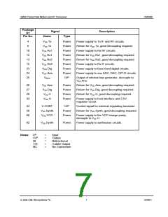
8
9
I/P
11
14
16
43
44
45
46
47
O/P
O/P
I/P
DAC3
O/P
O/P
I/P
DAC2
Spare D/A output.
ADC5
Spare A/D input.
ADC4
I/P
Spare A/D input.
OP2T
O/P
Uncommitted op-amp 2 output, internally
connected to ADC3.
48
49
50
OP2N
OP2P
OP1T
I/P
I/P
Uncommitted op-amp 2 negative input.
Uncommitted op-amp 2 positive input.
O/P
Uncommitted op-amp 1 output, internally
connected to ADC2.
51
52
53
54
55
OP1N
OP1P
I/P
I/P
Uncommitted op-amp 1 negative input.
Uncommitted op-amp 1 positive input.
Master clock input from external TCXO.
DAC1 output to control TCXO.
REFCLK
I/P
TCXO-CNTL
TCXO-TEMP
O/P
I/P
A/D input to measure TCXO temperature,
internally connected to ADC1.
56
57
59
61
63
64
LOCLKN
LOCLK
I/P
I/P
Inverted input from the RF Oscillator circuit.
Input from the RF Oscillator circuit.
MAINPLL
AUXPLL
IFCLK
O/P
O/P
I/P
Main PLL output, connect to external filter.
Aux PLL output, connect to external filter.
Input from the IF Oscillator circuit.
PA-TEMP
I/P
A/D input to measure PA temperature, internally
connected to ADC0.
ã 2004 CML Microsystems Plc
5
D/990/1

 CMLMICRO [ CML MICROCIRCUITS ]