GMSK Packet Data Modem and RF Transceiver
CMX990
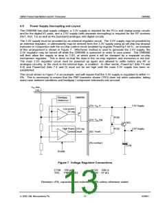
L6
VDD
H
3.3V
2.5V
L5
L4
L3
L2
L1
VDD VCO
VDD DIG
VDD Synth
VDD Plane for RX2 & ANA
VDD Plane for RX1 & TX
C7
C6
C5
C4
C3
C2
VSS RX1
VSS RX2
VSS Synth
VSS ANA
GND Plane for:
GND
VSS DIG
GND for:
VSS
H
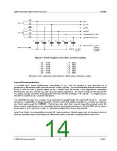
Figure 8 Power Supply Connections and De-coupling
C2 10 nF
C3 10 nF
C4 10 nF
C5 10 nF
C6 10 nF
C7 10 nF
L1 TBA
L2 TBA
L3 TBA
L4 TBA
L5 TBA
L6 TBA
Resistors ±5%, capacitors and inductors ±20% unless otherwise stated.
Layout Recommendations
To achieve good noise performance, decoupling of VBIAS and all supplies is very important as is
protection of the receive path from extraneous in-band signals. It is recommended that the printed circuit
board is laid out with a ground plane in the CMX990 area to provide a low impedance connection
between the VSS pins and all V and VBIAS decoupling capacitors. As shown in Figure 8 the ground for
VSS digital signals should be keDpDt separate from that used for analogue / RF signals. The digital ground
should be routed back to a suitable star point.
The CMX990 package has a copper area connected to ground under the main body of the IC. This pad
should be connected to analogue ground. It will be noted that caution should be exercised over placing
any tracks underneath the CMX990. Further any vias other than ground should be avoided under the
device unless manufacturers can guarantee that the exposed ground pad on the CMX990 will not cause
shorts while a good electrical contact is maintained between the device and ground.
Apart from these recommendations normal RF layout practices should apply such as keeping tracks as
short as possible, equal track lengths on differential inputs, care with coupling between tracks etc.
ã 2004 CML Microsystems Plc
14
D/990/1

 CMLMICRO [ CML MICROCIRCUITS ]