GMSK Packet Data Modem and RF Transceiver
CMX990
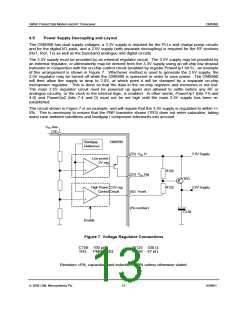
4.5
Power Supply Decoupling and Layout
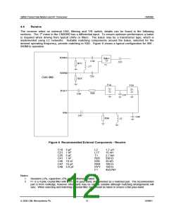
The CMX990 has dual supply voltages: a 3.3V supply is required for the PLLs and charge pump circuits
and for the digital I/O pads, and a 2.5V supply (with separate decoupling) is required for the RF sections
(Rx1, Rx2, Tx) as well as the baseband analogue and digital circuits.
The 3.3V supply must be provided by an external regulator circuit. The 2.5V supply may be provided by
an external regulator, or alternatively may be derived from the 3.3V supply using an off-chip low dropout
transistor in conjunction with the on-chip control circuit (enabled by register PowerUp1 bit 5) - an example
of this arrangement is shown in Figure 7. Whichever method is used to generate the 2.5V supply, the
2.5V regulator may be turned off while the CMX990 is quiescent in order to save power. The CMX990
will then allow the supply to drop to 2.0V, at which point it will be clamped by a separate on-chip
micropower regulator. This is done so that the data in the on-chip registers and memories is not lost.
The main 2.5V regulator circuit must be powered up again and allowed to settle before any RF or
analogue circuitry, or the clock to the internal logic, is enabled. In other words, PowerUp1 (bits 7-6 and
4-0) and PowerUp2 (bits 7-4 and 0) must not be set high until the main 2.5V supply has been re-
established.
The circuit shown in Figure 7 is an example, and will require that the 3.3V supply is regulated to within +/-
5%. This is necessary to ensure that the PNP transistor shown (TR3) does not enter saturation, taking
worst case ambient conditions and bandgap / component tolerances into account.
VDD Ana
(24)
Bandgap
CMX990
Reference
(33) VDD
H
3.3V Supply
Low power
2V reg
-
+
R126
R125
(23) VDD Dig
TR3
High Power 2.5V reg
Control Circuit
2.5V Supply
-
(42) Vcont
+
(Pin number)
C158
Enable
Figure 7 Voltage Regulator Connections
C158 100 µF
TR3 PMBT4403
R125 330 W
R126 47 kW
Resistors ±5%, capacitors and inductors ±20% unless otherwise stated.
ã 2004 CML Microsystems Plc
13
D/990/1

 CMLMICRO [ CML MICROCIRCUITS ]