V.22 bis Modem with AT Commands
CMX866
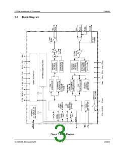
1.3
Signal List
CMX866
D1/D6
Signal
Name
Description
Pin No.
Type
XTALN
O/P
I/P
The output of the on-chip Xtal oscillator inverter.
1
2
XTAL/CLOCK
The input to the oscillator inverter from the Xtal
circuit or external clock source.
N/C
N/C
~
~
Reserved for future use. Connect this pin to
DVSS.
3
4
5
Reserved for future use. Connect this pin to
DVSS.
RDRVN
O/P
Relay drive output, low resistance pull down to
DVSS when active and medium resistance pull
up to DVDD when inactive.
DVSS
RD
Power
I/P
6
7
8
The negative supply rail for the digital on-chip
blocks.
Schmitt trigger input to the Ring signal detector.
Connect to DVSS if Ring Detector not used.
RT
BI
Open drain output and Schmitt trigger input
forming part of the Ring signal detector.
Connect to DVDD if Ring Detector not used.
RESETN
I/P
Schmitt trigger input to an active-low reset pin.
Connect to DVDD if no external reset signal
used
9
RXAFB
RXBN
O/P
I/P
The output of the Rx Input Amplifier.
10
11
An alternative, switched inverting input to the
Rx Input Amplifier, used to increase the
amplifier gain for the detection of on-hook
signals. If this input is not required, leave the
pin disconnected.
RXAN
RXA
I/P
I/P
12
13
The inverting input to the Rx Input Amplifier
The non-inverting input to the Rx Input
Amplifier. If this pin is to be connected to VBIAS
then it should also be decoupled to AVSS locally.
AVSS
VBIAS
Power
O/P
14
15
The negative supply rail for the analogue on-
chip blocks.
Internally generated bias voltage of
approximately AVDD /2, except when the device
is in Powersave or 'Zero-Power' modes, when
VBIAS will discharge to AVSS. This pin should be
decoupled to AVSS by a capacitor mounted
close to the device pins.
TXAN
TXA
O/P
O/P
16
17
The inverted output of the Tx Output Buffer.
The non-inverted output of the Tx Output Buffer.
ã 2004 CML Microsystems Plc
4
D/866/4

 CMLMICRO [ CML MICROCIRCUITS ]