EP9312
Universal Platform SOC Processor
2
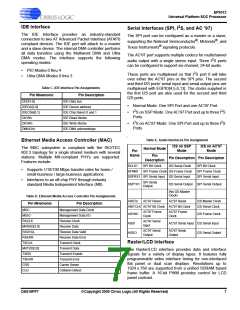
IDE Interface
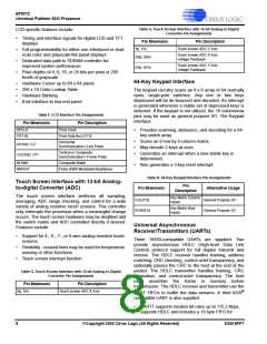
Serial Interfaces (SPI, I S, and AC ’97)
The IDE Interface provides an industry-standard
connection to two AT Advanced Packet Interface (ATAPI)
compliant devices. The IDE port will attach to a master
and a slave device. The internal DMA controller performs
all data transfers using the Multiword DMA and Ultra
DMA modes. The interface supports the following
operating modes:
The SPI port can be configured as a master or a slave,
®
®
supporting the National Semiconductor , Motorola , and
®
Texas Instruments signaling protocols.
The AC'97 port supports multiple codecs for multichannel
2
audio output with a single stereo input. Three I S ports
can be configured to support six-channel, 24-bit audio.
•
•
PIO Modes 0 thru 4
2
These ports are multiplexed so that I S port 0 will take
Ultra DMA Modes 0 thru 3
over either the AC'97 pins or the SPI pins. The second
and third I2S ports' serial input and serial output pins are
multiplexed with EGPIO[4,5,6,13]. The clocks supplied in
the first I2S port are also used for the second and third
I2S ports.
Table C. IDE Interface Pin Assignments
Pin Mnemonic
Pin Description
DD[15-0]
IDE Data bus
•
•
Normal Mode: One SPI Port and one AC’97 Port
IDEDA[2-0]
IDECSn[0,1]
DIORn
IDE Device address
IDE Chip Select 0 and 1
IDE Read Strobe
2
2
I S on SSP Mode: One AC’97 Port and up to three I S
Ports
2
2
DIOWn
IDE Write Strobe
•
I S on AC’97 Mode: One SPI Port and up to three I S
Ports
DMACKn
IDE DMA acknowledge
‘
Table E. Audio Interfaces Pin Assignment
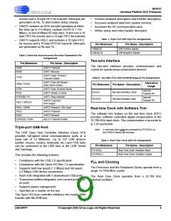
Ethernet Media Access Controller (MAC)
I2S on SSP
Mode
I2S on AC'97
Mode
The MAC subsystem is compliant with the ISO/TEC
802.3 topology for a single shared medium with several
stations. Multiple MII-compliant PHYs are supported.
Features include:
Normal Mode
Pin
Name
Pin
Description
Pin Description Pin Description
SCLK1
SPI Bit Clock
I2S Serial Clock
SPI Bit Clock
•
•
Supports 1/10/100 Mbps transfer rates for home /
small-business / large-business applications
SFRM1 SPI Frame Clock I2S Frame Clock
SSPRX1 SPI Serial Input I2S Serial Input
SPI Serial
SPI Frame Clock
SPI Serial Input
Interfaces to an off-chip PHY through industry
standard Media Independent Interface (MII)
SSPTX1
I2S Serial Output SPI Serial Output
Output
(No I2S Master
Clock)
Table D. Ethernet Media Access Controller Pin Assignments
ARSTn
AC'97 Reset
AC'97 Reset
I2S Master Clock
I2S Serial Clock
Pin Mnemonic
Pin Description
ABITCLK AC'97 Bit Clock AC'97 Bit Clock
MDC
Management Data Clock
AC'97 Frame
Clock
AC'97 Frame
Clock
ASYNC
ASDI
I2S Frame Clock
MDIO
Management Data I/O
Receive Clock
RXCLK
MIIRXD[3:0]
RXDVAL
RXERR
TXCLK
MIITXD[3:0]
TXEN
AC'97 Serial
Input
AC'97 Serial Input I2S Serial Input
Receive Data
AC'97 Serial
Output
AC'97 Serial
I2S Serial Output
Output
Receive Data Valid
Receive Data Error
Transmit Clock
Transmit Data
ASDO
Raster/LCD Interface
The Raster/LCD interface provides data and interface
signals for a variety of display types. It features fully
programmable video interface timing for non-interlaced
flat panel or dual scan displays. Resolutions up to
1024 x 768 are supported from a unified SDRAM based
frame buffer. A 16-bit PWM provides control for LCD
panel contrast.
Transmit Enable
Transmit Error
TXERR
CRS
Carrier Sense
CLD
Collision Detect
DS515PP7
©Copyright 2005 Cirrus Logic (All Rights Reserved)
7

 CIRRUS [ CIRRUS LOGIC ]