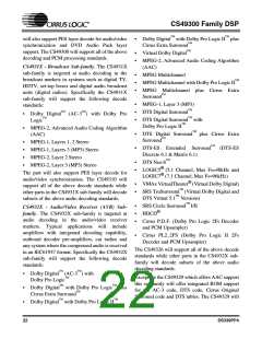
CS49300 Family DSP
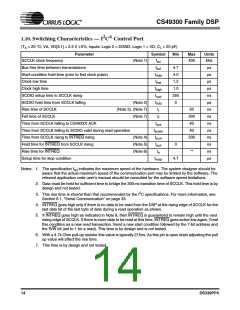
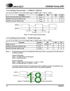
1.12. Switching Characteristics — CMPDAT, CMPCLK
(TA = 25 °C; VA, VD[3:1] = 2.5 V 5%; Inputs: Logic 0 = DGND, Logic 1 = VD, CL = 20 pF)
Parameter
Symbol
Min
Max
Unit
Serial compressed data clock CMPCLK period
Tcmpclk
-
27
MHz
CMPDAT setup before CMPCLK high
CMPDAT hold after CMPCLK high
Tcmpsu
Tcmphld
5
3
-
-
ns
ns
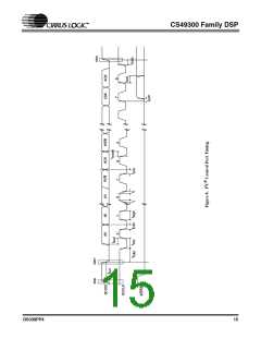
CMPCLK
CMPDAT
Tcm psu
Tcm phld
Tcm pclk
Figure 10. Serial Compressed Data Timing
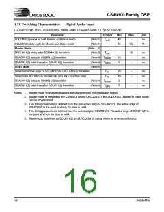
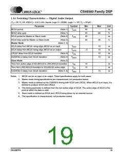
1.13. Switching Characteristics — Parallel Data Input
(TA = 25 °C; VA, VD[3:1] = 2.5 V 5%; Inputs: Logic 0 = DGND, Logic 1 = VD, CL = 20 pF)
Parameter
Symbol
Min
Max
Unit
CMPCLK Period
Tcmpclk
4*DCLK + 10
ns
ns
ns
DATA[7:0] setup before CMPCLK high
DATA[7:0] hold after CMPCLK high
Tcmpsu
Tcmphld
10
10
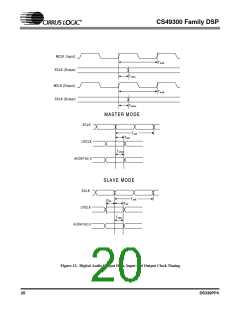
Notes: 1. Certain timing parameters are normalized to the DSP clock, DCLK, in nanoseconds. The DSP clock can
be defined as follows:
External CLKIN Mode:
DCLK == CLKIN/4 before and during boot
DCLK == CLKIN after boot
Internal Clock Mode:
DCLK == 10MHz before and during boot, i.e. DCLK == 100ns
DCLK == 65 MHz after boot, i.e. DCLK == 15.4ns
It should be noted that DCLK for the internal clock mode is application specific. The application code
users guide should be checked to confirm DCLK for the particular application.
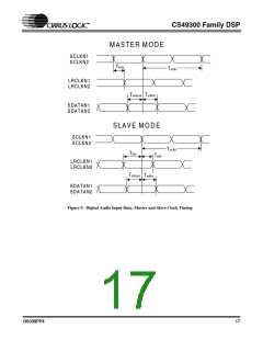
CM PCLK
DATA[7:0]
Tcm psu
Tcm phld
Tcm pclk
Figure 11. Parallel Data Timing (when not in a parallel control mode)
18
DS339PP4

 CIRRUS [ CIRRUS LOGIC ]