CS4397
8.0 CONTROL PORT INTERFACE
The control port is used to load all the internal settings of the CS4397. The operation of the control port
may be completely asynchronous to the audio sample rate. However, to avoid potential interference prob-
lems, the control port pins should remain static if no operation is required.
2
The control port has 2 modes: SPI and I C, with the CS4397 operating as a slave device in both modes. If
2
I C operation is desired, AD0/CS should be tied to VD or DGND. If the CS4397 ever detects a high to low
transition on AD0/CS after power-up, SPI mode will be selected.
8.1 SPI Mode
In SPI mode, CS is the CS4397 chip select signal, CCLK is the control port bit clock, CDIN is the input
data line from the microcontroller, CDOUT is the data output and the chip address is 0010000. The data
is clocked on the rising edge of CCLK.
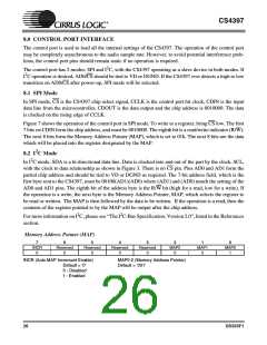
Figure 7 shows the operation of the control port in SPI mode. To write to a register, bring CS low. The first
7 bits on CDIN form the chip address, and must be 0010000. The eighth bit is a read/write indicator (R/W).
The next 8 bits form the Memory Address Pointer (MAP), which is set to 01h. The next 8 bits are the data
which will be placed into the register designated by the MAP.
8.2 I2C Mode
2
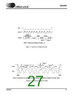
In I C mode, SDA is a bi-directional data line. Data is clocked into and out of the part by the clock, SCL,
with the clock to data relationship as shown in Figure 3. There is no CS pin. Pins AD0 and AD1 form the
partial chip address and should be tied to VD or DGND as required. The 7-bit address field, which is the
first byte sent to the CS4397, must be 00100(AD1)(AD0) where (AD1) and (AD0) match the setting of the
AD0 and AD1 pins. The eighth bit of the address byte is the R/W bit (high for a read, low for a write). If
the operation is a write, the next byte is the Memory Address Pointer, MAP, which selects the register to
be read or written. The MAP is then followed by the data to be written. If the operation is a read, then the
contents of the register pointed to by the MAP will be output after the chip address.
2
2
For more information on I C, please see “The I C-Bus Specification: Version 2.0”, listed in the References
section.
Memory Address Pointer (MAP)
7
INCR
0
6
Reserved
0
5
Reserved
0
4
Reserved
0
3
Reserved
0
2
MAP2
0
1
MAP1
0
0
MAP0
1
INCR (Auto MAP Increment Enable)
Default = ‘0’
MAP0-2 (Memory Address Pointer)
Default = ‘001’
0 - Disabled
1 - Enabled
26
DS333F1

 CIRRUS [ CIRRUS LOGIC ]