CS4397
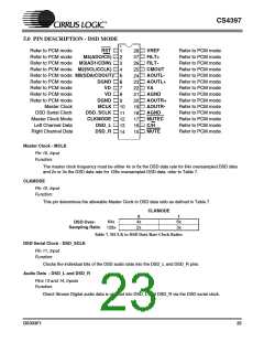
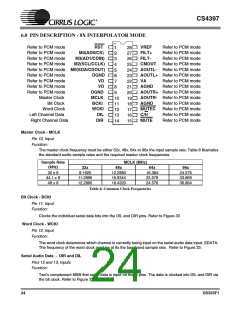
6.0 PIN DESCRIPTION - 8X INTERPOLATOR MODE
Refer to PCM mode
Refer to PCM mode
Refer to PCM mode
Refer to PCM mode
RST
M4(AD0/CS)
M3(AD1/CDIN)
M2(SCL/CCLK)
VREF
FILT+
FILT-
Refer to PCM mode
Refer to PCM mode
Refer to PCM mode
1
2
3
4
5
6
7
8
28
27
26
25
24
23
22
21
20
19
18
17
16
15
CMOUT Refer to PCM mode
AOUTL- Refer to PCM mode
AOUTL+ Refer to PCM mode
VA
AGND
AOUTR+ Refer to PCM mode
AOUTR- Refer to PCM mode
AGND
MUTEC
C/H
Refer to PCM mode M0(SDA/CDOUT)
Refer to PCM mode
Refer to PCM mode
Refer to PCM mode
Refer to PCM mode
Master Clock
Bit Clock
Word Clock
Left Channel Data
Right Channel Data
DGND
VD
Refer to PCM mode
Refer to PCM mode
VD
DGND
MCLK
BCKI
WCKI
DIL
9
10
11
12
13
14
Refer to PCM mode
Refer to PCM mode
Refer to PCM mode
Refer to PCM mode
DIR
MUTE
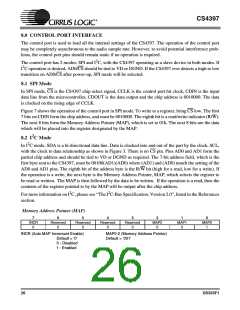
Master Clock - MCLK
Pin 10, Input
Function:
The master clock frequency must be either 32x, 48x, 64x or 96x the input sample rate. Table 8 illustrates
the standard audio sample rates and the required master clock frequencies.
Sample Rate
(kHz)
MCLK (MHz)
32x
48x
64x
96x
32 x 8
44.1 x 8
48 x 8
8.1920
11.2896
12.2880
12.2880
16.9344
18.4320
16.384
22.579
24.576
24.576
33.869
36.864
Table 8. Common Clock Frequencies
Bit Clock - BCKI
Pin 11, Input
Function:
Clocks the individual serial data bits into the DIL and DIR pins. Refer to Figure 33
Word Clock - WCKI
Pin 12, Input
Function:
The word clock determines which channel is currently being input on the serial audio data input, SDATA.
The frequency of the word clock must be at 8x the baseband sample rate. Refer to Figure 33.
Serial Audio Data - DIR and DIL
Pins 12 and 13, Inputs
Function:
Two's complement MSB-first serial data is input on these pins. The data is clocked into DIL and DIR via
the bit clock. Refer to Figure 33.
24
DS333F1

 CIRRUS [ CIRRUS LOGIC ]