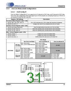
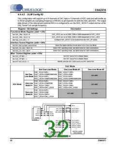
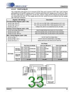
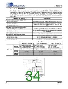
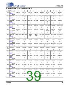
CS42416
4.6
Control Port Description and Timing
The control port is used to access the registers, allowing the CS42416 to be configured for the desired op-
erational modes and formats. The operation of the control port may be completely asynchronous with re-
spect to the audio sample rates. However, to avoid potential interference problems, the control port pins
should remain static if no operation is required.
The control port has two modes: SPI and I²C, with the CS42416 acting as a slave device. SPI mode is se-
lected if there is a high-to-low transition on the AD0/CS pin after the RST pin has been brought high. I²C
mode is selected by connecting the AD0/CS pin through a resistor to VLC or DGND, thereby permanently
selecting the desired AD0 bit address state.
4.6.1
SPI Mode
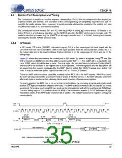
In SPI mode, CS is the CS42416 chip-select signal; CCLK is the control port bit clock (input into the
CS42416 from the microcontroller); CDIN is the input data line from the microcontroller, and CDOUT is
the output data line to the microcontroller. Data is clocked in on the rising edge of CCLK and out on the
falling edge.
Figure 21 shows the operation of the control port in SPI mode. To write to a register, bring CS low. The
first seven bits on CDIN form the chip address and must be 1001111. The eighth bit is a read/write indi-
cator (R/W), which should be low to write. The next eight bits form the Memory Address Pointer (MAP),
which is set to the address of the register that is to be updated. The next eight bits are the data which will
be placed into the register designated by the MAP. During writes, the CDOUT output stays in the Hi-Z
state. It may be externally pulled high or low with a 47 kΩ resistor, if desired.
There is a MAP auto-increment capability, enabled by the INCR bit in the MAP register. If INCR is a zero,
the MAP will stay constant for successive read or writes. If INCR is set to a 1, the MAP will auto-increment
after each byte is read or written, allowing block reads or writes of successive registers.
To read a register, the MAP has to be set to the correct address by executing a partial write cycle which
finishes (CS high) immediately after the MAP byte. The MAP auto increment bit (INCR) may be set or not,
as desired. To begin a read, bring CS low, send out the chip address and set the read/write bit (R/W) high.
The next falling edge of CCLK will clock out the MSB of the addressed register (CDOUT will leave the high
impedance state). If the MAP auto-increment bit is set to 1, the data for successive registers will appear
consecutively.
CS
C C L K
C H IP
C H IP
M A P
DATA
A D D R E SS
ADDRESS
1001111
1001111
LSB
MSB
byte 1
R/W
R/W
C D IN
b yte n
High Impedance
LSB
LSB
MSB
MSB
C D O U T
MAP = Memory Address Pointer, 8 bits, MSB first
Figure 21. Control Port Timing in SPI Mode
DS602F1
35

 CIRRUS [ CIRRUS LOGIC ]