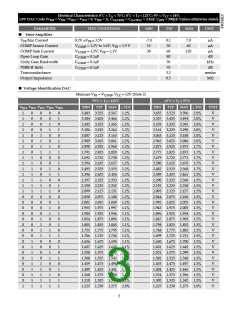
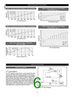
Electrical Characteristics: 0˚C < TA < 70˚C; 0˚C < TJ < 125˚C; 9V < VCC < 14V;
2.0V DAC Code (VID4 = VID3 =VID2 = VID1 = 0, VID0 = 1), CGATE(H) = CGATE(L) = 3.3nF, COFF = 390pF; Unless otherwise stated.
PARAMETER
TEST CONDITIONS
MIN
TYP
MAX
UNIT
ꢀ General Electrical Specifications
V
CC Monitor Start Threshold
CC Monitor Stop Threshold
7.9
7.6
8.4
8.1
8.9
8.6
V
V
V
Hysteresis
CC Supply Current
Start - Stop
No Load on GATE(H), GATE(L)
0.15
0.30
12
0.60
20
V
V
mA
Note 1: All pins are rated 2kV except for the VREF pin (Pin 5) which is typically rated at 800V.
Note 2: The IC power dissipation in a typical application with VCC = 12V, switching frequency fSW = 250kHz, 50nc
MOSFETs and RθJA = 115°C/W yields an operating junction temperature rise of approximately 52°C, and a junction tem-
perature of 77°C with an ambient temperature of 25°C.
Note 3: Guaranteed by design, not 100% tested in production.
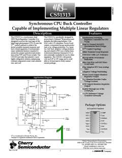
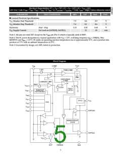
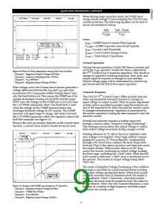
Block Diagram
C
OFF
V
FB
COMP
1.10V
PWM COMP
-
+
-
EA
-
OFF
TIME
+
DISCHARGE
COMP
-
CURRENT LIMIT
R
+
+
-
86mV
V
OUT
-
Q
+
-
0.25V
FAULT
LATCH
S
BANDGAP
REFERENCE
V
REF
V
ID0
V
ID1
UVLO
V
CC
DAC
V
V
ID2
ID3
GATE(H)
V
ID4
NONOVERLAP
LOGIC
+
-
GATE(L)
+
-
V
CC
OVP
PWRGD
Gnd
5

 CHERRY [ CHERRY SEMICONDUCTOR CORPORATION ]