Absolute Maximum Ratings
Operating Junction Temperature, TJ . . . . . . . . . . . . . . . . . . . . . . . . . . . . . . . . . . . . . . . . . . . . . . . . . . . . . . . . . . . . . . . . 150°C
Lead Temperature Soldering
Reflow (SMD styles only) . . . . . . . . . . . . . . . . . . . . . . . . . . . . . . . . . . . . . . . . . . . . .60 sec. max above 183°C, 230°C peak
Storage Temperature Range, TS . . . . . . . . . . . . . . . . . . . . . . . . . . . . . . . . . . . . . . . . . . . . . . . . . . . . . . . . . . . . . . −65° to 150°C
ESD Susceptibility (Note 1) . . . . . . . . . . . . . . . . . . . . . . . . . . . . . . . . . . . . . . . . . . . . . . . . . . . . . . . . . . . . . . . . . . . . . . . . . . 2kV
VMAX
VMIN
ISOURCE
ISINK
Pin Symbol
VREF
VCC
Pin Name
Bandgap Reference Voltage
IC Power Input
6V
16V
-0.3V
-0.3V
1mA
N/A
1mA
1.5A Peak
200mA DC
COMP
Compensation Pin
6V
6V
-0.3V
-0.3V
1mA
1mA
5mA
1mA
VFB, VOUT, VID0-4
Voltage Feedback Input, Output
Voltage Sense Pin, Voltage
ID DAC Inputs
COFF
Off-Time Pin
6V
16V
-0.3V
-0.3V
1mA
1.5APeak
200mA DC 200mA DC
50mA
1.5A Peak
GATE(H), GATE(L) High-Side, Low Side FET Drivers
PWRGD
OVP
Gnd
Power-Good Output
Overvoltage Protection
Ground
6V
15V
0V
-0.3V
-0.3V
0V
1mA
30mA
1.5A Peak
200mA DC
30mA
1mA
N/A
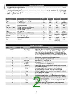
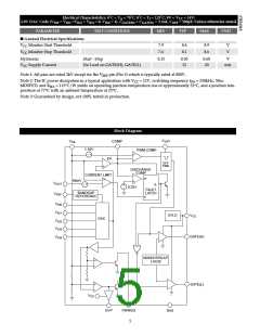
Package Pin Description
PACKAGE PIN #
1,2,3,4,6
PIN SYMBOL
FUNCTION
VIDO – VID4
Voltage ID DAC inputs. These pins are internally pulled up to
5.65V if left open. VID4 selects the DAC range. When VID4 is
high (logic one), the Error Amp reference range is 2.125V to
3.525V with 100mV increments. When VID4 is low (logic zero),
the Error amp reference voltage is 1.325V to 2.075V with 50mV
increments.
9
VCC
Input power supply pin for the internal circuitry.
Decouple with filter capacitor to Gnd.
10
11
12
14
GATE(H)
Gnd
GATE(L)
PWRGD
High side switch FET driver pin
Ground pin.
Low side synchronous FET driver pin.
Power-Good Output. Open collector output drives low when
VFB is out of regulation.
16
15
COMP
COFF
Error amp output. PWM comparator inverting input.
A capacitor to Gnd provides error amp compensation.
Off-Time Capacitor Pin. A capacitor from this pin to Gnd sets
the off time for the regulator
8
7
VOUT
VFB
Current limit comparator inverting input.
Error amp inverting input, PWM comparator non-inverting
input, current limit comparator non-inverting input, PWRGD
and OVP comparator input.
5
VREF
OVP
Bandgap Reference Voltage. It can be used to generate other
regulated output voltages.
13
Overvoltage protection pin. Goes high when overvoltage
condition is detected on VFB
.
2

 CHERRY [ CHERRY SEMICONDUCTOR CORPORATION ]