Application Information: continued
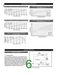
Slope Compensation
threshold, the current sense comparator allows the fault
latch to be set. This causes the regulator to stop switching.
The V2TM control method uses a ramp signal, generated by
the ESR of the output capacitors, that is proportional to the
ripple current through the inductor. To maintain regula-
tion, the V2TM control loop monitors this ramp signal,
through the PWM comparator, and terminates the switch
on-time.
During this over current condition, the CS51313 stays off
for the time it takes the COMP pin capacitor to discharge
to its lower 0.25V threshold. As soon as the COMP pin
reaches 0.25V, the Fault latch is reset (no overcurrent con-
dition present) and the COMP pin is charged with a 30µA
current source to a voltage 1.1V greater than the VFB volt-
age. Only at this point the regulator attempts to restart nor-
mally. The CS51313 will operate initially with a duty cycle
whose value depends on how low the VFB voltage was
during the overcurrent condition (whether hiccup mode
was due to excessive current or hard short). This protec-
tion scheme minimizes thermal stress to the regulator com-
ponents, input power supply, and PC board traces, as the
over current condition persists. Upon removal of the over-
load, the fault latch is cleared, allowing normal operation
to resume.
The stringent load transient requirements of modern
microprocessors require the output capacitors to have very
low ESR. The resulting shallow slope presented to the
PWM comparator, due to the very low ESR, can lead to
pulse width jitter and variation caused by both random or
synchronous noise.
Adding slope compensation to the control loop, avoids
erratic operation of the PWM circuit, particularly at lower
duty cycles and higher frequencies, where there is not
enough ramp signal, and provides a more stable switch-
point.
Overvoltage Protection
The scheme that prevents that switching noise prematurely
triggers the PWM circuit consists of adding a positive volt-
age slope to the output of the Error Amplifier (COMP pin)
during an off-time cycle.
Overvoltage protection (OVP) is provided as result of the
normal operation of the V2TM control topology and requires
no additional external components. The control loop
responds to an overvoltage condition within 200ns, caus-
ing the top MOSFET to shut off, disconnecting the regula-
tor from its input voltage. This results in a “crowbar”
action to clamp the output voltage and prevents damage to
the load. The regulator will remain in this state until the
overvoltage condition ceases or the input voltage is pulled
low. Additionally, a dedicated Overvoltage protection
(OVP) output pin (pin 13) is provided in the CS51313. The
OVP signal will go high (overvoltage condition), if the out-
put voltage (VCC(CORE)) exceeds the regulation voltage by
8.5% of the voltage set by the particular DAC code. The
OVP pin can source up to 25mA of current that can be
used to drive an SCR to crowbar the power supply.
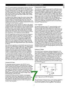
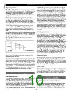
The circuit that implements this function is shown in
Figure 12.
16
COMP
C
2
COMP
CS51313
GATE(L)
R
C
1
R
1
12
To Synchronous FET
Figure 12: Small RC filter provides the proper voltage ramp at the
beginning of each on-time cycle.
Power-Good Circuit
The Power-Good pin (pin 14) is an open-collector signal
consistent with TTL DC specifications. It is externally
pulled up, and is pulled low (below 0.3V) when the regula-
tor output voltage typically exceeds ± 8.5% of the nominal
output voltage. Maximum output voltage deviation before
Power-Good is pulled low is ± 12%.
The ramp waveform is generated through a small RC filter
that provides the proper voltage ramp at the beginning of
each on-time cycle. The resistors R1 and R2 in the circuit of
Figure 12 form a voltage divider from the GATE(L) output,
superimposing a small artificial ramp on the output of the
error amplifier. It is important that the series combination
R1/R2 is high enough in resistance not to load down and
negatively affect the slew rate on the GATE(L) pin.
Output Enable
On/off control of the regulator outputs can be implement-
ed by pulling the COMP pins low. It is required to pull the
COMP pins below the 1.1V PWM comparator offset volt-
age in order to disable switching on the GATE drivers.
Protection and Monitoring Features
Overcurrent Protection
CS51313-based VCC(CORE)
Buck Regulator Design Example
A loss-less hiccup mode current limit protection feature is
provided, requiring only the COMP capacitor to imple-
ment. The CS51313 provides overcurrent protection by
sensing the current through a “Droop” resistor, using an
internal current sense comparator. The comparator com-
pares the voltage drop across the “Droop” resistor to an
internal reference voltage of 86mV (typical).
Step 1: Definition of the design specifications
In computer motherboard applications the input voltage
comes from the “silver box” power supply. 5V ± 5% is
used for conversion to output voltage, and 12V ± 5% is
used for the external NFET gate voltage and circuit bias.
If the voltage drop across the “Droop” resistor exceeds this
10

 CHERRY [ CHERRY SEMICONDUCTOR CORPORATION ]