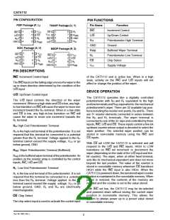
CAT5112
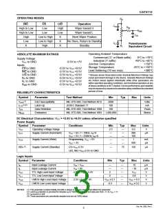
OPERATING MODES
RH
INC
High to Low
High to Low
High
CS
U/D
High
Low
X
Operation
Wiper toward H
CH
Rwi
Low
Low
RWB
CW
Wiper toward L
Low to High
Low to High
High
Store Wiper Position
No Store, Return to Standby
Standby
Low
X
CL
Potentiometer
Equivalent Circuit
X
X
RL
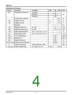
Operating Ambient Temperature
ABSOLUTE MAXIMUM RATINGS
Commercial (‘C’ or Blank suffix)
Industrial (‘I’ suffix)
Junction Temperature
Storage Temperature
Lead Soldering (10 sec max)
0°C to +70°C
-40°C to +85°C
+150°C
-65°C to +150°C
+300°C
Supply Voltage
VCC to GND
Inputs
-0.5V to +7V
CS to GND
INC to GND
U/D to GND
RH to GND
RL to GND
RWB to GND
-0.5V to VCC +0.5V
-0.5V to VCC +0.5V
-0.5V to VCC +0.5V
-0.5V to VCC +0.5V
-0.5V to VCC +0.5V
-0.5V to VCC +0.5V
* Stresses above those listed under Absolute Maximum Ratings may
cause permanent damage to the device. Absolute Maximum Ratings
are limited values applied individually while other parameters are
within specified operating conditions, and functional operation at any
of these conditions is NOT implied. Device performance and reliability
maybeimpairedbyexposuretoabsoluteratingconditionsforextended
periods of time.
RELIABILITY CHARACTERISTICS
Symbol
Parameter
Test Method
Min
Typ
Max
Units
(1)
VZAP
ESD Susceptibility
Latch-Up
MIL-STD-883, Test Method 3015
2000
100
Volts
mA
(1)(2)
ILTH
JEDEC Standard 17
TDR
Data Retention
Endurance
MIL-STD-883, Test Method 1008
MIL-STD-883, Test Method 1003
100
Years
Stores
NEND
1,000,000
DC Electrical Characteristics: VCC = +2.5V to +6.0V unless otherwise specified
Power Supply
Symbol Parameter
Conditions
Min
2.5
Typ
—
Max
6.0
Units
V
VCC
ICC1
Operating Voltage Range
Supply Current (Increment)
VCC = 6V, f = 1MHz, IW=0
VCC = 6V, f = 250kHz, IW=0
—
—
—
—
200
100
µA
ICC2
Supply Current (Write)
Programming, VCC = 6V
VCC = 3V
—
—
—
—
1
mA
500
µA
(2)
ISB1
Supply Current (Standby)
CS=VCC-0.3V
—
75
150
µA
U/D, INC=VCC-0.3V or GND
Logic Inputs
Symbol Parameter
Conditions
Min
Typ
Max
Units
IIH
Input Leakage Current
VIN = VCC
—
—
—
—
—
—
—
10
–10
µA
µA
V
IIL
Input Leakage Current
VIN = 0V
—
VIH1
VIL1
VIH2
VIL2
TTL High Level Input Voltage
TTL Low Level Input Voltage
CMOS High Level Input Voltage
CMOS Low Level Input Voltage
4.5V ≤ VCC ≤ 5.5V
2
0
VCC
0.8
V
2.5V ≤ VCC ≤ 6V
VCC x 0.7
-0.3
VCC + 0.3
VCC x 0.2
V
V
NOTES: (1) This parameter is tested initially and after a design or process change that affects the parameter.
(2) Latch-up protection is provided for stresses up to 100mA on address and data pins from –1V to VCC + 1V
(3) IW=source or sink
(4) These parameters are periodically sampled and are not 100% tested.
Doc. No. 2002, Rev. L
3

 CATALYST [ CATALYST SEMICONDUCTOR ]