LH0032 / LH0032C
CORPORATION
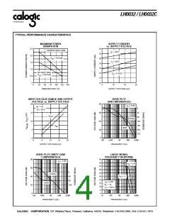
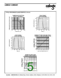
Although this approach offers the shortest settling time, the
falling edge exhibits overshoot up to 30% lasting 200 to
300ns. Figure 4 shows the typical pulse response.
waveform is shown in Figure 6. The settling time to 1% final
value is actually superior to the first method of compensation.
However, the LH0032 suffers slow settling thereafter to 0.1%
accuracy at the falling edge, and nearly four times as much at
the rising edge, compared to the previous scheme. Note,
however, that the falling edge ringing is considerably reduced.
Furthermore, the slew rate is consistently superior using this
compensation because of the smaller value of Miller
capacitance CC required.
If obtaining minimum ringing at the falling edge is the primary
objective, a slight modification to the above is recommended.
It is based on the same circuit as that of Figure 1.
The values of the unity gain compensation capacitors CC and
CA should be modified to 5pF and 1000pF, respectively.
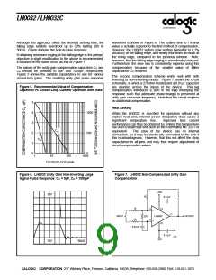
Figure 5 shows the suitable capacitance to use for various
closed-loop gains. The resulting unity gain pulse response
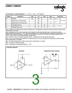
The second compensation scheme works well with both
inverting or non-inverting modes. Figure 7 shows the circuit
schematic, in which a 270ohm resistor and a 0.01µF capacitor
are shunted across the inputs of the device. This lag
compensation introduces a zero in the loop modifying the
response such that adequate phase margin is preserved at
unity gain crossover frequency. Note that the circuit requires
no additional compensation.
Figure 5. Recommended Value of Compensation
Capacitor vs Closed-Loop Gain for Optimum Slew Rate
5
Heat Sinking
4
3
2
1
0
1000
500
0
While the LH0032 is specified for operation without any
explicit heat sink, internal power dissipation does cause a
significant temperature rise.
Improved bias current
performance can thus be obtained by limiting this temperature
rise with a small heat sink such as the Thermalloy No. 2241 or
C
equivalent.
The case of the device has no internal
C
connection, so it may be electrically connected to the sink if
this is advantageous. However, that this will affect the stray
capacitance to all pins and may thus require adjustment of
circuit compensation values.
C
A
1
10
100
1000
CLOSED LOOP GAIN
Figure 6. LH0032 Unity Gain Non-Inverting Large
Signal Pulse Response: CC = 5pF, CA = 1000pF
Figure 7. LH0032 Non-Compensated Unity Gain
Compensation
+15V
10V
1k
0.01µF
1k
12
LH0032
10
5
6
_
+
11
INPUT
OUTPUT
270
1k
0.01µF
0.01µF
-15V
10V
50nS
CALOGIC CORPORATION, 237 Whitney Place, Fremont, California 94539, Telephone: 510-656-2900, FAX: 510-651-1076

 CALOGIC [ CALOGIC, LLC ]