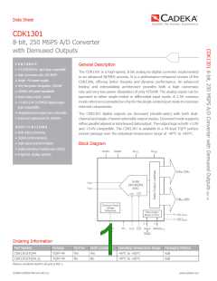
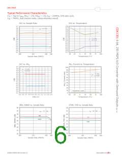
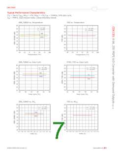
Data Sheet
Electrical Characteristics
(T = T to T , AV = +5V, OV = +5V, ƒ = 250MHz, 50% duty cycle,
Min
A
Max
CC
DD
clk
ƒ = 70MHz, dual channel mode; unless otherwise noted)
IN
symbꢀꢁ
pꢂꢃꢂmꢄꢅꢄꢃ
cꢀꢆdꢇꢅꢇꢀꢆꢈ
Mꢇꢆ
tyꢉ
Mꢂx
uꢆꢇꢅꢈ
Power Supply Requirements
AVcc
Analog Voltage Supply(2)
Digital Voltage Supply(2)
Current(1)
4.75
2.75
5.0
5.25
5.25
110
5.5
V
OVDD
V
85
mA
mA
AIcc
Current Power-down(1)
4.8
+25°C
OIDD
Current
OVDD = 3.0V, 10pF load
Single Mode
35
55
mA
mA
mA
mW
Parallel Mode
Interleave Mode
Power Dissipation(1)
55
425
550
Common Mode Reference Output
Voltage(1)
2.44
2.5
84
2.56
V
Voltage Tempcp
ppm/°C
kΩ
Open Impedance
IOUT = ±50µA
1.07
47.5
PSRR
Power Supply Rejection Ratio
mV/V
Clock and Reset Inputs (Differential and Single-Ended)
VDIFF
VIHD
VILD
VCMD
VIH
Differental Signal Amplitude(2)
Differental High Input Voltage(2)
Differental Low Input Voltage(2)
Differental Common Mode Input(2)
Single-Ended High Input Voltage(1)
Single-Ended Low Input Voltage(2)
High Input Current(1)
400
1.4
0
mVpp
V
AVcc
3.9
V
1.2
1.8
0
4.1
V
V
VIL
1.2
V
IIH
VID = 1.5V
VID = 1.5V
-100
-100
43
43
+100
+100
µA
µA
IIL
Low Input Current(1)
Power Down and Mode Control Inputs (Single-Ended)
High Input Voltage(2)
2.0
0
AVcc
1.0
V
Low Input Voltage(2)
V
Max Input Current Low(1)
Max Input Current High <4.0V(1)
Digital Outputs
-100
-100
0.5
50
+100
+100
µA
µA
Logic “1“ Voltage(1)
IOH = -0.5mA
OVDD-2.0
V
Logic “0“ Voltage(1)
IOL = +1.6mA
0.2
V
OVDD = 3V, 10pF load
OVDD = 5V, 10pF load
OVDD = 3V, 10pF load
OVDD = 5V, 10pF load
3.3/3.0
2.3/1.9
1.2/1.0
0.7/0.6
ns
ns
ns
ns
TR/TF Data
TR/TF DCLK
nꢀꢅꢄꢈ:
1. 100% production tested at +25°C.
2. Parameter is guaranteed (but not tested) by design and characterization data.
©2008 CADEKA Microcircuits LLC
www.cadeka.com
5

 CADEKA [ CADEKA MICROCIRCUITS LLC. ]