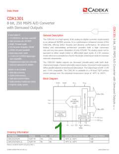
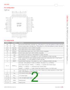
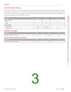
Data Sheet
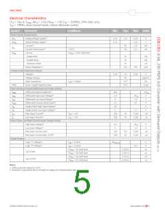
Electrical Characteristics
(T = T to T , AV = +5V, OV = +5V, ƒ = 250MHz, 50% duty cycle,
Min
A
Max
CC
DD
clk
ƒ = 70MHz, dual channel mode; unless otherwise noted)
IN
symbꢀꢁ
pꢂꢃꢂmꢄꢅꢄꢃ
cꢀꢆdꢇꢅꢇꢀꢆꢈ
Mꢇꢆ
tyꢉ
Mꢂx
uꢆꢇꢅꢈ
Resolution
8
bits
DC Performance
+25°C, ƒIN = 1KHz(1)
-40°C to +85°C, ƒIN = 1KHz(2)
+25°C, ƒIN = 1KHz(1)
-40°C to +85°C, ƒIN = 1KHz(2)
@250 MSPS, ƒIN = 1KHz(1)
-0.68
-0.95
±0.4
±0.7
±1.2
±1.4
0.68
0.95
LSB
LSB
LSB
LSB
DLE
Differential Linearity Error
±1.90
±2.15
ILE
Integral Linearity Error
No Missing Codes
Guaranteed
Analog Input
VCM
Input Voltage Range
Input Common Mod(2)
Input Bias Current
Input Resistance
with respect to VIN-
±512
2.5
13
mVpp
V
2.0
3.0
+25°C
µA
+25°C
50
kΩ
Input Capacitance
Input Bandwidth
Gain Error(1)
+25°C
5
pF
+25°C (-3dB of FS)
+25°C
350
MHz
%FS
LSB
LSB
-7.5
-5
+3.5
+5
Offset Error(1)
+25°C
PSRR
Offset Power Supply Rejection Ratio
AVcc = 5V ±0.25V
<1
Timing Characteristics
Conversion Rate(2)
25
7
250
8
MSPS
ns
tpd1
Output Delay (Clock-to-Data)(2)
Output Delay Tempco
Aperture Delay Time
Aperture Jitter Time
-40°C to +85°C
9.4
16
ps/°C
ns
tap
0.3
2.0
ps-RMS
Pipeline Delay (Latency)
Single Channel Mode
Demuxed Interleaved Mode
Demuxed Parallel Mode
Channel B
2.5
2.5
Cycle
Cycle
2.5
3.5
Cycle
Cycle
Channel A
CLK to DCLKOUT Delay Time
Single Channel Mode(2)
Dual Channel Mode(2)
Output Delay (Clock to DClock)
tpd2
tpd3
5.0
5.6
5.18
5.73
18.1
5.3
5.9
ns
ns
ps/°C
Dynamic Performance
ƒIN = 70MHz, +25°C(1)
ƒIN = 70MHz, -40°C to +85°C(2)
ƒIN = 70MHz,+25°C(1)
ƒIN = 70MHz, -40°C to +85°C(2)
ƒIN = 70MHz, +25°C(1)
ƒIN = 70MHz, -40°C to +85°C(2)
ƒIN = 70MHz, +25°C(1)
6.4
7.0
6.8
Bits
Bits
dB
ENOB
SNR
Effective Number of Bits
6.25
44.3
42.6
46.1
45.4
-47
Signal-to-Noise Ratio
dB
-41.5
-40.3
dB
THD
Total Harmonic Distortion
Signal-to-Noise and Distortion
-45.5
43.7
42.8
dB
40.2
39.3
dB
SINAD
ƒIN = 70MHz, -40°C to +85°C(2)
dB
nꢀꢅꢄꢈ:
1. 100% production tested at +25°C.
2. Parameter is guaranteed (but not tested) by design and characterization data.
©2008 CADEKA Microcircuits LLC
www.cadeka.com
4

 CADEKA [ CADEKA MICROCIRCUITS LLC. ]