Data Sheet
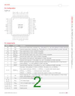
Pin Configuration
TQFP-44
CDK1301
Pin Assignments
Pin No.
40
Pin Name
Description
VIN+
VIN-
Non-inverted analog input; nominally 1Vpp; 100k pullup to Vcc and 100k pulldown to AGND, internally
Inverted analog input; nominally 1Vpp; 100k pullup to Vcc and 100k pulldown to AGND, internally
Data output bank A; 3V/5V LVCMOS compatible
39
16-9
19-26
28
DA0–DA7
DB0–DB7
DCLKOUT
DCLKOUT
CLK
Data output bank B; 3V/5V LVCMOS compatible
Non-inverted data output clock; 3v/5v 3V/5V LVCMOS compatible
Inverted data output clock; 3V/5V LVCMOS compatible
27
4
Non-inverted clock input pin; 100k pulldown to AGND, internally
3
CLK
Inverted clock input pin; 17.5k pullup to V and 7.5k pulldown to AGND, internally
cc
RESET synchronizes the data sampling and data output bank relationship when in dual channel
mode (DMODE1 = 0); 100k pulldown to AGND, internally
5
6
RESET
RESET
Inverted RESET input pin; 17.5k pullup to V and 7.5 pulldown to AGND, internally
cc
Internally: 100k pulldown to AGND on DMODE1 50k pullup to V on DMODE2
cc
Data output mode pins: DMODE1 = 0, DMODE2 = 0: parallel dual channel output
DMODE1 = 0, DMODE2 = 1: interleaved dual channel output
32, 31
DMODE1,2
DMODE1 = 1, DMODE2 = x: single channel data output on bank a (125 MSPS max)
Power-Down pin; PD = 1 for Power-Down mode. Outputs set to high impedance in Power-Down
mode; 100k pulldown to AGND, internally
2
PD
37
VCM
2.5V common mode voltage reference output
35, 36,
42, 43
AVCC
+5V analog supply
7, 17, 30
OVDD
+3V/+5V digital output supply
1, 33, 34,
38, 41, 44
AGND
DGND
Analog ground
Digital ground
8, 18, 29
©2008 CADEKA Microcircuits LLC
www.cadeka.com
2

 CADEKA [ CADEKA MICROCIRCUITS LLC. ]