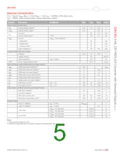
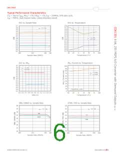
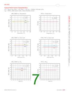
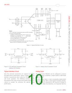
Data Sheet
selected transformer does not exhibit core saturation at
the full-scale voltage. Proper termination of the input is
important for input signal purity. A small capacitor across
the input attenuates kickback noise from the internal track-
and-hold.
Common-Mode Voltage Reference Circuit
The CDK1301 has an on-board common-mode voltage
reference circuit (V ). It is 2.5V and is capable of driving
CM
50µA loads typically. The circuit is commonly used to drive
the center tap of the RF transformer in fully differential
applications. For single-ended applications, this output
can be used to provide the level shifting required for the
single-to-differential converter conversion circuit. Bypass
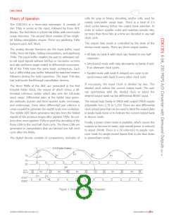
Figure 6 illustrates a solution (based on operational ampli-
fiers) that can be used if a DC-coupled single-ended input
is desired.
V
to AGND by external 0.01µF capacitor, as shown in
CM
Figure 3 on the previous page.
Clock Input
The clock input on the CDK1301 can be driven by
either a single-ended or double-ended clock circuit and
can handle TTL, PECL, and CMOS signals. When operating
at high sample rates it is important to keep the pulse width
of the clock signal as close to 50% as possible. For TTL/
CMOS single- ended clock inputs, the rise time of the signal
also becomes an important consideration.
Figure 6. DC-Coupled Single-Ended to Differential
Conversion (power supplies and bypassing are not shown)
Digital Outputs
The output circuitry of the CDK1301 has been designed
to be able to support three separate output modes. The
demuxed (double-wide) mode supports either parallel
alignedorinterleaveddataoutput.Thesingle-channelmode
is not demuxed and can support direct output at speeds up
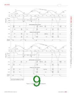
to 125 MSPS. The output format is straight binary (Table 1).
Input Protection
All I/O pads are protected with an on-chip protection cir-
cuit. This circuit provides ESD robustness and prevents
latchup under severe discharge conditions without degrad-
ing analog transmission times.
Table 1. Output Data Format
Power Supplies and Grounding
aꢆꢂꢁꢀg iꢆꢉꢊꢅ
+FS
oꢊꢅꢉꢊꢅ cꢀdꢄ D7–D0
1111 1111
The CDK1301 is operated from a single power supply in
the range of 4.75V to 5.25V. Normal operation is suggest-
ed to be 5.0V. All power supply pins should be bypassed
as close to the package as possible. The analog and digital
grounds should be connected together with a ferrite bead
as shown in the typical interface circuit and as close to the
ADC as possible.
+FS - 1 LSB
+1 FS
1111 111Ø
1000 000Ø
-FS + 1 LSB
-FS
0000 000Ø
0000 0000
Ø indicates the flickering bit between logic 0 and 1
The data output mode is set using the DMODE and
1
DMODE inputs(pins32&31respectively).Table2describes
the mode switching options.
Power-Down Mode
2
To save on power, the CDK1301 incorporates a power-
down function. This function is controlled by the signal on
pin PD. When pin PD is set high, the CDK1301 enters the
power-down mode. All outputs are set to high impedance.
In the powerdown mode the CDK1301 dissipates 24mW
typically.
Table 2. Output Data Modes
oꢊꢅꢉꢊꢅ Mꢀdꢄ
DMoDe1
DMoDe2
Parallel Dual Channel Output
Interleaved Dual Channel Output
0
0
1
0
1
X
Single Channel Data Output
(Bank A only 125 MSPS max)
©2008 CADEKA Microcircuits LLC
www.cadeka.com
11

 CADEKA [ CADEKA MICROCIRCUITS LLC. ]