Data Sheet
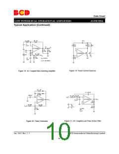
LOW POWER DUAL OPERATIONAL AMPLIFIERS
AS358/358A
Electrical Characteristics (Continued)
Note 3: The input common-mode voltage of either input signal voltage should not be allowed to go negatively by
more than 0.3V (at 25oC). The upper end of the common-mode voltage range is V -1.5V (at 25oC), but either or
CC
both inputs can go to +36V without damages, independent of the magnitude of the V
.
CC
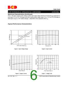
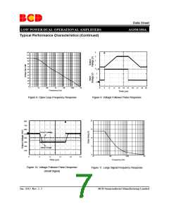
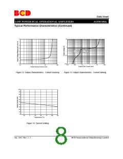
Typical Performance Characteristics
15
10
5
20
18
16
14
12
10
8
NEGATIVE
POSITIVE
6
4
2
0
0
0
5
10
15
-25
0
25
50
75
100
125
Temperature (oC)
Power Supply Voltage (+VDC
)
Figure 4. Input Voltage Range
Figure 5. Input Current
120
105
90
1.0
0.9
0.8
0.7
0.6
0.5
0.4
0.3
0.2
0.1
0.0
RL=2KΩ
RL=20KΩ
75
60
0
8
16
24
32
40
0
5
10
15
20
25
30
35
40
Supply Voltage (V)
Power Supply Voltage (V)
Figure 6. Supply Current
Jan. 2013 Rev. 2. 2
Figure 7. Voltage Gain
BCD Semiconductor Manufacturing Limited
6

 BCDSEMI [ BCD SEMICONDUCTOR MANUFACTURING LIMITED ]