Data Sheet
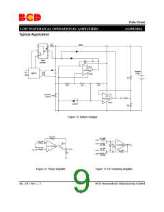
LOW POWER DUAL OPERATIONAL AMPLIFIERS
AS358/358A
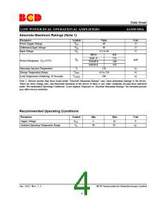
Absolute Maximum Ratings (Note 1)
Parameter
Symbol
Value
40
Unit
V
VCC
Power Supply Voltage
Differential Input Voltage
Input Voltage
VID
VIC
40
V
-0.3 to 40
V
DIP-8
SOIC-8
TSSOP-8
MSOP-8
830
550
500
470
PD
Power Dissipation (TA=25oC)
mW
oC
oC
oC
TJ
Operating Junction Temperature
Storage Temperature Range
150
-65 to 150
260
TSTG
TLEAD
Lead Temperature (Soldering, 10 Seconds)
Note 1: Stresses greater than those listed under "Absolute Maximum Ratings" may cause permanent damage to the device.
These are stress ratings only, and functional operation of the device at these or any other conditions beyond those indicated
under "Recommended Operating Conditions" is not implied. Exposure to "Absolute Maximum Ratings" for extended periods
may affect device reliability.
Recommended Operating Conditions
Parameter
Symbol
VCC
Min
3
Max
36
Unit
V
Supply Voltage
oC
Ambient Operating Temperature Range
TA
-40
85
Jan. 2013 Rev. 2. 2
BCD Semiconductor Manufacturing Limited
4

 BCDSEMI [ BCD SEMICONDUCTOR MANUFACTURING LIMITED ]