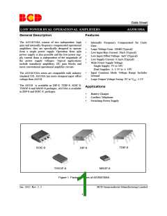
Data Sheet
LOW POWER DUAL OPERATIONAL AMPLIFIERS
AS358/358A
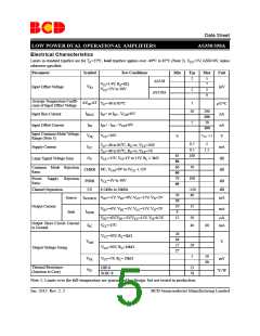
Electrical Characteristics
Limits in standard typeface are for TA=25oC, bold typeface applies over -40oC to 85oC (Note 2), VCC=5V, GND=0V, unless
otherwise specified.
Parameter
Symbol
Test Conditions
Min
Typ
Max
Unit
2
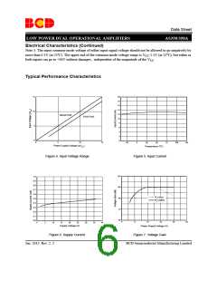
5
7
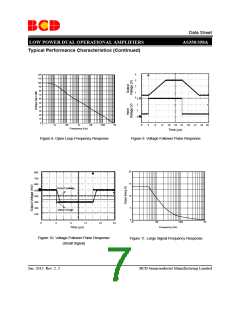
3
5
AS358
VO=1.4V, RS=0Ω,
VCC=5V to 30V
VIO
Input Offset Voltage
mV
2
AS358A
Average Temperature Coeffi-
cient of Input Offset Voltage
TA=-40 to 85oC
μV/oC
ΔVIO/ΔT
IBIAS
IIO
7
20
200
200
30
IIN+ or IIN-, VCM=0V
Input Bias Current
Input Offset Current
nA
5
IIN+ - IIN-, VCM=0V
VCC=30V
nA
V
100
Input Common Mode Voltage
Range (Note 3)
V
-1.5
VIR
0
CC
TA=-40 to 85oC, RL=∞, VCC=30V
TA=-40 to 85oC, RL=∞, VCC=5V
0.7
0.5
2
ICC
Supply Current
mA
1.2
85
80
60
60
70
60
100
GV
VCC=15V, VO=1V to 11V, RL ≥ 2kΩ
Large Signal Voltage Gain
dB
dB
70
Common Mode Rejection
Ratio
DC, VCM=0V to (VCC-1.5)V
CMRR
100
Power Supply Rejection
Ratio
VCC=5V to 30V
PSRR
CS
dB
dB
Channel Separation
Source
f=1kHz to 20kHz
-120
40
20
20
10
5
ISOURCE VIN+=1V, VIN-=0V, VCC=15V, VO=2V
mA
Output Current
Sink
15
VIN+=0V, VIN-=1V, VCC=15V, VO=2V
ISINK
mA
V
IN+=0V,VIN-=1V,VCC=15V, VO=0.2V
12
50
40
μA
Output Short Circuit Current
to Ground
ISC
VCC=15V
60
mA
26
26
27
27
VCC=30V, RL=2kΩ
VOH
V
28
5
V
CC=30V, RL=10kΩ
Output Voltage Swing
20
VOL
VCC=5V, RL= 10kΩ
mV
30
Thermal Resistance
(Junction to Case)
DIP-8
53
78
oC/W
θJC
SOIC-8
Note 2: Limits over the full temperature are guaranteed by design, but not tested in production.
Jan. 2013 Rev. 2. 2 BCD Semiconductor Manufacturing Limited
5

 BCDSEMI [ BCD SEMICONDUCTOR MANUFACTURING LIMITED ]