Preliminary Datasheet
BOOST CONTROLLER
AP3039
For Input Hysteresis Voltage
=22μA*R1
Application Information
Operation
V
IN-HYSTERESIS
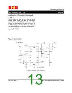
AP3039 is a boost DC-DC controller with adjustable
operation frequency. Current mode control scheme
provides excellent line and load regulation. Operation
can be best understood by referring to Figure 3.
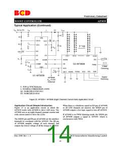
Over Voltage Protection
AP3039 has an over voltage protection (OVP) circuit.
The OV Pin is connected to the center tap of R3 and R4
resistor voltage-divider from the high voltage output to
GND. (see Figure 21). When the loop is open or the
output voltage becomes excessive in any case, result
the voltage on OV pin exceeds 1.25V, all functions of
AP3039 will be disabled, and the output voltage will
fall. OVP hysteresis is accomplished with an internal
22μA current source and the operation mode is the
same as UVLO. The formula for OVP can be expresses
as blow:
At the start of each oscillator cycle, the SR latch is set
and external power switch Q1 (see Figure 4) turns on
and the switch current will increase linearly. The
voltage on external sense resistor R (see Figure4),
CS
connected from CS pin to GND, is proportional to the
switch current. This voltage is added to a stabilizing
ramp and the result is fed into the non-inversion input
of the PWM comparator. When this non-inversion
input voltage exceeds inversion input voltage of PWM
comparator which is the output voltage of the error
amplifier EA, the SR latch is reset and the external
power switch turns off. The voltage level at inversion
input of PWM comparator sets the peak current level to
keep the output voltage in regulation. This voltage
level is the amplified signal of the voltage difference
between feedback voltage and reference voltage of
0.5V. So, a constant output current can be provided by
this operation mode.
For OVP Voltage
V
=1.25V*(R3+R4)/R4
OVP
For OVP Hysteresis Voltage
=22μA*R3
V
OVP-HYSTERESIS
Frequency Selection
An external resistor R , connected from RT pin to
T
GND, is used to set the operating frequency (see Figure
4). Operation frequency range is from 400kHz to
1MHz (see Table 1). High frequency operation
optimizes the regulator for the smallest component
size, while low frequency operation can reduce the
switch losses.
Input Under-Voltage Detector
AP3039 contains an Under Voltage Lock Out (UVLO)
circuit. Two resistors R1 and R2 are connected from
UVLO pin to ground and VIN pin respectively (see
Figure 4). The resistor divider must be designed such
that the voltage on the UVLO pin is higher than 1.25V
when VIN is in the desired operating range. If the
voltage on the pin is below under voltage threshold, all
functions of AP3039 are disabled, but the system will
remain in a low power standby state. UVLO hysteresis
is accomplished through an internal 22μA current
source which switched on or off 22μA current into the
impedance of the set-point divider. When the UVLO
threshold is exceeded, the current source is activated to
instantly raise the voltage on the UVLO pin. When the
UVLO pin voltage falls below the threshold the current
source is turned off, causing the voltage on the UVLO
pin to fall. The formula for UVLO can be expresses as
blow:
Table 1. Frequency Selection
Operating Frequency
Resistance of RT (kΩ)
(kHz)
147
95
400
600
68
800
51
1000
For Input Threshold Voltage
V
=1.25V*(R1+R2)/R2
IN_THRESHOLD
May 2008 Rev. 1. 0
BCD Semiconductor Manufacturing Limited
12

 BCDSEMI [ BCD SEMICONDUCTOR MANUFACTURING LIMITED ]