in the serial input bit stream. Table II describes the exact
relationship of input data to voltage output coding. Any
number of bits can precede the 20 bits to be loaded, since
only the last 20 will be transferred to the parallel DAC
register after Latch Enable (Pin6 <PCM1702P>, Pin7
<PCM1702U>, LE) has gone low.
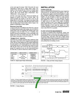
INSTALLATION
POWER SUPPLIES
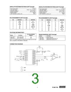
Refer to CONNECTION DIAGRAM for proper connection
of the PCM1702. The PCM1702 only requires a ±5V sup-
ply. Both positive supplies should be tied together at a single
point. Similarly, both negative supplies should be connected
together. No real advantage is gained by using separate
analog and digital supplies. It is more important that both
these supplies be as “clean” as possible to reduce coupling
of supply noise to the output. Power supply decoupling
capacitors should be used at each supply pin to maximize
power supply rejection, as shown in CONNECTION DIA-
GRAM regardless of how good the supplies are. Both
commons should be connected to an analog ground plane as
close to the PCM1702 as possible.
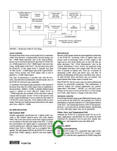
All DAC serial input data (Pin1, DATA) bit transfers are
triggered on positive clock (Pin2, CLOCK), edges. The
serial-to-parallel data transfer to the DAC occurs on the
falling edge of Latch Enable. The change in the output of the
DAC occurs at a rising edge of the 4th clock of the CLOCK
after the falling edge of Latch Enable. Refer to Figure 2 for
graphical relationships of these signals.
Maximum Clock Rate
A typical clock rate of 16.9MHz for the PCM1702 is derived
by multiplying the standard audio sample rate of 44.1kHz by
sixteen times (16X over-sampling) the standard audio word
bit length of 24 bits (44.1kHz x 16 x 24 = 16.9MHz). Note
that this clock rate accommodates a 24-bit word length, even
though only 20 bits are actually being used. The setup and
hold timing relationships are shown in Figure 3.
FILTER CAPACITOR REQUIREMENTS
As shown in CONNECTION DIAGRAM, various size
decoupling capacitors can be used, with no special tolerances
being required. The size of the offset decoupling capacitor is
not critical either, with larger values (up to 100µF) giving
slightlybetterSNRreadings.Allcapacitorsshouldbeasclose
to the appropriate pins of the PCM1702 as possible to reduce
noise pickup from surrounding circuitry.
“Stopped Clock” Operation
The PCM1702 is normally operated with a continuous clock
input signal. If the clock is to be stopped between input data
words, the last 20 bits shifted in are not actually shifted from
the serial register to the latched parallel DAC register until
Latch Enable goes low. Latch Enable must remain low until
after the first clock cycle of the next data word to insure
proper DAC operation. In any case, the setup and hold times
for Data and LE must be observed as shown in Figure 3.
> 40ns
Data Input
LSB
MSB
> 15ns > 15ns
Clock
Input
> 20ns
> 20ns
DIGITAL INPUT
ANALOG OUTPUT
CURRENT OUTPUT
1,048,576LSBs
1LSB
7FFFFHEX
00000HEX
80000HEX
Full Scale Range
NA
+Full Scale
Bipolar Zero –1LSB
–Full Scale
2.40000000mA
2.28882054nA
–1.19999771mA
0.00000000mA
+1.20000000mA
> 15ns
Latch
Enable
> 15ns
> One Clock Cycle
> One Clock Cycle
TABLE II. Digital Input/Output Relationships.
FIGURE 3. Setup and Hold Timing Diagram.
Clock
DATA "N"
1
2
3
4
12 13 14 15 16 17 18 19 20
1
Data
MSB
LSB
Latch
Enable
IOUT
N-1
N
NOTES : (1) If clock is stopped between input of 20-bit data words, "Latch" Enable (LE) must remain low until after the first clock cycle of the next 20-bit data
word stream. (2) Data format is binary two's complement (BTC). Individual data bits are clocked in on the corresponding positive clock edge. (3) Latch Enable
(LE) must remain low at least one clock cycle after going negative. (4) Latch Enable (LE) must be high for at least one clock cycle before going negative. (5)
IOUT changes on positive going edge of the 4th clock after negative going edge of Latch Enable (LE).
FIGURE 2. Timing Diagram.
®
7
PCM1702

 BB [ BURR-BROWN CORPORATION ]