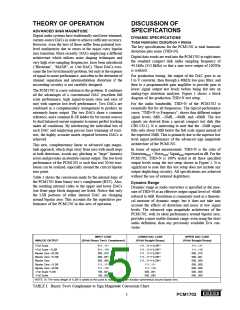
SPECIFICATIONS
All specifications at 25°C, ±VCC and +VDD = ±5V unless otherwise noted.
PCM1702P/U, -J, -K
TYP
PARAMETER
CONDITIONS
MIN
MAX
UNITS
Bits
RESOLUTION
20
DYNAMIC RANGE, THD + N at –60dB Referred to Full Scale, with A-weight
110
dB
DIGITAL INPUT
Logic Family
Logic Level: VIH
VIL
TTL/CMOS Compatible
+2.4
0
+VDD
0.8
V
V
IIH
IIL
VIH = +VDD
VIL = 0V
±10
±10
µA
µA
Data Format
Serial, MSB First, BTC(1)
12.5
Input Clock Frequency
20.0
MHz
TOTAL HARMONIC DISTORTION + N(2)
P/U
VO = 0dB
fS = 352.8kHz(3), f = 1002Hz(4)
fS = 352.8kHz(3), f = 1002Hz(4)
fS = 352.8kHz(3), f = 1002Hz(4)
fS = 352.8kHz(3), f = 1002Hz(4)
fS = 352.8kHz(3), f = 1002Hz(4)
fS = 352.8kHz(3), f = 1002Hz(4)
fS = 352.8kHz(3), f = 1002Hz(4)
fS = 352.8kHz(3), f = 1002Hz(4)
fS = 352.8kHz(3), f = 1002Hz(4)
–92
–82
–46
–96
–83
–48
–100
–84
–50
–88
–74
–40
–92
–76
–42
–96
–80
–44
dB
dB
dB
dB
dB
dB
dB
dB
dB
V
V
V
V
V
V
V
V
O = –20dB
O = –60dB
O = 0dB
O = –20dB
O = –60dB
O = 0dB
P/U, -J
P/U, -K
O = –20dB
O = –60dB
ACCURACY
Level Linearity
Gain Error
At –90dB Signal Level
±0.5
±0.5
±0.25
±25
±5
dB
%
%
±3
Bipolar Zero Error(5)
Gain Drift
0°C to 70°C
0°C to 70°C
ppm of FSR/°C
ppm of FSR/°C
minute
Bipolar Zero Drift
Warm-up Time
1
IDLE CHANNEL SNR(6)
Bipolar Zero, A-weighted Filter
110
120
dB
ANALOG OUTPUT
Output Range
Output Impedance
Settling Time
±1.2
1.0
200
mA
kΩ
ns
(±0.003% of FSR, 1.2mA Step)
Glitch Energy
No Glitch Around Zero
POWER SUPPLY REQUIREMENTS
Supply Voltage Range: +VCC = +VDD
–VCC = –VDD
Combined Supply Current: +ICC
Combined Supply Current: –ICC
Power Dissipation
+4.75
–4.75
+5.00
–5.00
+5.00
–25.00
150
+5.25
–5.25
+9.0
–41.0
250
V
V
mA
mA
mW
+VCC = +VDD = +5V
–VCC = –VDD = –5V
±VCC = ±VDD = ±5V
TEMPERATURE RANGE
Operating
Storage
–25
–55
+85
+125
°C
°C
NOTES: (1) Binary Two’s Complement coding. (2) Ratio of (DistortionRMS + NoiseRMS) / SignalRMS. (3) D/A converter sample frequency (8 x 44.1kHz; 8x oversampling).
(4) D/A converter output frequency (signal level). (5) Offset error at bipolar zero. (6) Measured using an OPA627 and 5kΩ feedback and an A-weighted filter.
The information provided herein is believed to be reliable; however, BURR-BROWN assumes no responsibility for inaccuracies or omissions. BURR-BROWN assumes
no responsibility for the use of this information, and all use of such information shall be entirely at the user’s own risk. Prices and specifications are subject to change
without notice. No patent rights or licenses to any of the circuits described herein are implied or granted to any third party. BURR-BROWN does not authorize or warrant
any BURR-BROWN product for use in life support devices and/or systems.
®
2
PCM1702

 BB [ BURR-BROWN CORPORATION ]