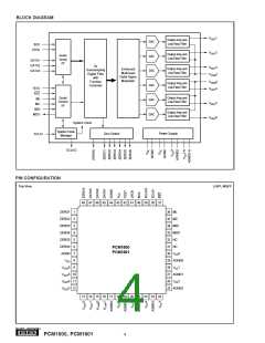
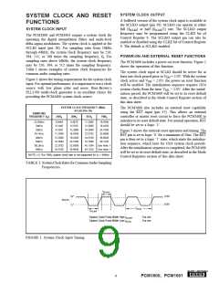
PIN ASSIGNMENTS
PIN
1
NAME
ZERO1
ZERO2
ZERO3
ZERO4
ZERO5
ZERO6
AGND
VCC
I/O
O
O
O
O
O
O
—
—
O
O
O
O
O
O
O
O
—
—
—
—
—
—
—
—
—
—
—
—
—
—
—
—
O
I
DESCRIPTION
Zero Data Flag for VOUT1.
2
Zero Data Flag for VOUT2.
3
Zero Data Flag for VOUT3.
4
Zero Data Flag for VOUT4.
5
Zero Data Flag for VOUT5.
6
Zero Data Flag for VOUT6.
7
Analog Ground
8
Analog Power Supply, +5V
9
VOUT
VOUT
VOUT
VOUT
VOUT
VOUT
6
5
4
3
2
1
Voltage Output of Audio Signal Corresponding to Rch on DATA3.
Voltage Output of Audio Signal Corresponding to Lch on DATA3.
Voltage Output of Audio Signal Corresponding to Rch on DATA2.
Voltage Output of Audio Signal Corresponding to Lch on DATA2.
Voltage Output of Audio Signal Corresponding to Rch on DATA1.
Voltage Output of Audio Signal Corresponding to Lch on DATA1.
Common Voltage Output. This pin should be bypassed with a 10µF capacitor to AGND.
Common Voltage Output. This pin should be bypassed with a 10µF capacitor to AGND.
Analog Ground
10
11
12
13
14
15
16
17
18
19
20
21
22
23
24
25
26
27
28
29
30
31
32
33
34
35
36
37
38
39
40
41
42
43
44
45
46
47
48
VCOM
VCOM
AGND6
VCC
AGND5
VCC
AGND4
VCC
AGND3
VCC
AGND2
VCC
AGND1
VCC
AGND0
VCC
2
1
6
Analog Power Supply, +5V
Analog Ground
5
Analog Power Supply, +5V
Analog Ground
4
Analog Power Supply, +5V
Analog Ground
3
Analog Power Supply, +5V
Analog Ground
2
Analog Power Supply, +5V
Analog Ground
1
Analog Power Supply, +5V
Analog Ground
0
Analog Power Supply, +5V
NC
NC
No Connection. Must be open.
No Connection. Must be open.
MDO
MDI
Serial Data Output for Function Register Control Port(3)
Serial Data Input for Function Register Control Port(1)
Shift Clock for Function Register Control Port(1)
Latch Enable for Function Register Control Port(1)
System Reset, Active LOW(1)
MC
I
ML
I
RST
I
SCLKI
SCLKO
BCK
I
System Clock In. Input frequency is 256, 384, 512 or 768fS.(2)
Buffered Clock Output. Output frequency is 256, 384, 512, or 768fS and one-half of 256, 384, 512, or 768fS.
Shift Clock Input for Serial Audio Data(2)
Left and Right Clock Input. This clock is equal to the sampling rate, fS.(2)
Test Pin. This pin should be connected to DGND.(1)
Digital Power Supply, +3.3V
O
I
LRCK
TEST
VDD
I
—
—
—
I
DGND
DATA1
DATA2
DATA3
ZEROA
Digital Ground for +3.3V
Serial Audio Data Input for VOUT1 and VOUT2(2)
Serial Audio Data Input for VOUT3 and VOUT4(2)
Serial Audio Data Input for VOUT5 and VOUT6(2)
Zero Data Flag. Logical “AND” of ZERO1 through ZERO6.
I
I
I
NOTES: (1) Schmitt-Trigger input with internal pull-down, 5V tolerant. (2) Schmitt-Trigger input, 5V tolerant. (3) Tri-state output.
®
5
PCM1600, PCM1601

 BB [ BURR-BROWN CORPORATION ]