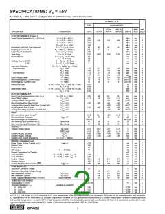
SPECIFICATIONS: VS = +5V
RF = 499Ω, RL = 100Ω to VS/2, and G = +2, (Figure 2 for AC performance only), unless otherwise noted.
OPA681P, U, N
GUARANTEED
TYP
0
°
C to
–40
°
C to
MIN/
TEST
MAX LEVEL(1)
PARAMETER
CONDITIONS
+25°C
+25°C(2)
70°C(3)
+85°C(3)
UNITS
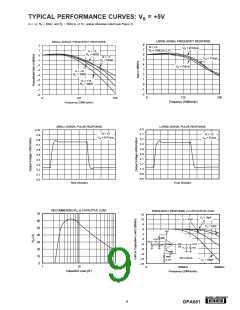
AC PERFORMANCE (Figure 2)
Small-Signal Bandwidth (VO = 0.5Vp-p)
G = +1, RF = 649Ω
G = +2, RF = 499Ω
G = +5, RF = 360Ω
G = +10, RF = 200Ω
G = +2, VO < 0.5Vp-p
F = 649Ω, VO < 0.5Vp-p
G = +2, VO = 2Vp-p
G = +2, 2V Step
G = +2, VO = 0.5V Step
G = +2, VO = 2V Step
G = +2, VO = 2V Step
G = +2, VO = 2V Step
250
225
180
165
100
0.4
200
830
1.5
2.0
14
MHz
MHz
MHz
MHz
MHz
dB
MHz
V/µs
ns
typ
min
typ
C
B
C
C
B
B
C
B
C
C
C
C
180
140
110
23
typ
Bandwidth for 0.1dB Gain Flatness
Peaking at a Gain of +1
Large-Signal Bandwidth
Slew Rate
50
2
35
4
min
max
typ
min
typ
typ
typ
typ
R
700
680
570
Rise/Fall Time
ns
ns
ns
Settling Time to 0.02%
0.1%
9
Harmonic Distortion
2nd Harmonic
G = +2, f = 5MHz, VO = 2Vp-p
RL = 100Ω to VS/2
–70
–72
–72
–73
2.2
12
–68
–70
–65
–68
3
–67
–70
–65
–67
3.4
14
–63
–68
–62
–67
3.6
15
dBc
dBc
dBc
max
max
max
max
max
max
max
B
B
B
B
B
B
B
RL ≥ 500Ω to VS/2
3rd Harmonic
RL = 100Ω to VS/2
RL ≥ 500Ω to VS/2
dBc
Input Voltage Noise
Non-Inverting Input Current Noise
Inverting Input Current Noise
f > 1MHz
f > 1MHz
f > 1MHz
nV/√Hz
pA/√Hz
pA/√Hz
14
18
15
18
19
DC PERFORMANCE(4)
Open-Loop Transimpedance Gain (ZOL
Input Offset Voltage
Average Offset Voltage Drift
Non-Inverting Input Bias Current
Average Non-Inverting Input Bias Current Drift
Inverting Input Bias Current
)
VO = VS/2, RL = 100Ω to VS/2
100
±1
60
±5
53
±6.0
+15
+75
–300
±25
51
±7
kΩ
mV
µV/°C
µA
nA/°C
µA
nA/°C
min
max
max
max
max
max
max
A
A
B
A
B
A
B
V
V
V
V
V
CM = 2.5V
CM = 2.5V
CM = 2.5V
CM = 2.5V
CM = 2.5V
+20
+95
–350
±35
–175
+40
+65
±5
±20
Average Inverting Input Bias Current Drift
VCM = 2.5V
–125
INPUT
Least Positive Input Voltage(5)
Most Positive Input Voltage(5)
Common-Mode Rejection Ratio (CMRR)
Non-Inverting Input Impedance
Min Inverting Input Resistance (RI )
Max Inverting Input Resistance (RI )
1.5
3.5
51
100 || 2
46
46
1.6
3.4
45
1.7
3.3
44
1.8
3.2
44
V
V
dB
kΩ || pF
Ω
Ω
max
min
min
typ
min
max
A
A
A
C
A
A
VCM = VS/2
Open-Loop
Open-Loop
38
53
36
55
35
60
OUTPUT
Most Positive Output Voltage
No Load
L = 100Ω to VS/2
No Load
4
3.9
1
1.1
150
–110
0.03
3.8
3.7
1.2
1.3
110
–75
3.7
3.6
1.3
1.4
110
–70
3.5
3.4
1.5
1.6
60
V
V
V
min
min
max
max
min
min
typ
A
A
A
A
A
A
C
R
Least Positive Output Voltage
RL = 100Ω to VS/2
V
Current Output, Sourcing
Current Output, Sinking
Closed-Loop Output Impedance
V
V
O = VS/2
O = VS/2
mA
mA
Ω
–50
G = +2, f = 100kHz
DISABLE (Disable Low)
Power Down Supply Current (+VS)
Disable Time
Enable Time
Off Isolation
Output Capacitance in Disable
Turn On Glitch
Turn Off Glitch
Enable Voltage
Disable Voltage
VDIS = 0
–270
100
25
65
4
±50
±20
3.3
1.8
100
µA
ns
ns
dB
pF
mV
mV
V
typ
typ
typ
typ
typ
typ
typ
min
max
typ
C
C
C
C
C
C
C
A
A
C
G = +2, 5MHz
G = +2, RL = 150Ω, VIN = VS /2
G = +2, RL = 150Ω, VIN = VS /2
3.5
1.7
3.6
1.6
3.7
1.5
V
µA
Control Pin Input Bias Current (DIS)
VDIS = 0
POWER SUPPLY
Specified Single-Supply Operating Voltage
Max Single-Supply Operating Voltage
Max Quiescent Current
Min Quiescent Current
Power Supply Rejection Ratio (–PSRR)
5
V
V
mA
mA
dB
typ
max
max
min
typ
C
A
A
A
C
12
5.3
4.1
12
5.4
3.7
12
5.4
3.6
V
V
S = +5V
S = +5V
10.0
10.0
48
Input Referred
TEMPERATURE RANGE
Specification: P, U, N
–40 to +85
°C
typ
C
Thermal Resistance, θJA
Junction-to-Ambient
P
U
N
8-Pin DIP
SO-8
SOT23-6
100
125
150
°C/W
°C/W
°C/W
typ
typ
typ
C
C
C
NOTES: (1) Test levels: (A) 100% tested at 25°C. Over temperature limits by characterization and simulation. (B) Limits set by characterization and simulation.
(C) Typical value only for information. (2) Junction temperature = ambient for 25°C guaranteed specifications. (3) Junction temperature = ambient at low temperature
limit: junction temperature = ambient +23°C at high temperature limit for over temperature guaranteed specifications. (4) Current is considered positive out-of-node.
VCM is the input common-mode voltage. (5) Tested < 3dB below minimum specified CMR at ±CMIR limits.
®
3
OPA681

 BB [ BURR-BROWN CORPORATION ]