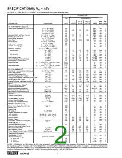
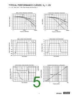
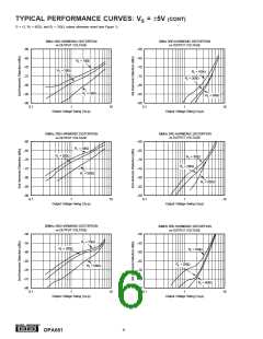
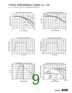
SPECIFICATIONS: VS = ±5V
RF = 402Ω, RL = 100Ω, and G = +2, (Figure 1 for AC performance only), unless otherwise noted.
OPA681P, U, N
GUARANTEED
TYP
0
°
C to
–40
°
C to
MIN/
TEST
MAX LEVEL(1)
PARAMETER
CONDITIONS
+25°C
+25°C(2)
70°C(3)
+85°C(3)
UNITS
AC PERFORMANCE (Figure 1)
Small-Signal Bandwidth (VO = 0.5Vp-p)
G = +1, RF = 453Ω
G = +2, RF = 402Ω
G = +5, RF = 261Ω
G = +10, RF = 180Ω
G = +2, VO = 0.5Vp-p
RF = 453, VO = 0.5Vp-p
G = +2, VO = 5Vp-p
G = +2, 4V Step
G = +2, VO = 0.5V Step
G = +2, 5V Step
G = +2, VO = 2V Step
G = +2, VO = 2V Step
280
220
185
180
90
0.4
150
2100
1.7
2.0
12
MHz
MHz
MHz
MHz
MHz
dB
MHz
V/µs
ns
typ
min
typ
C
B
C
C
B
B
C
B
C
C
C
C
220
210
190
45
typ
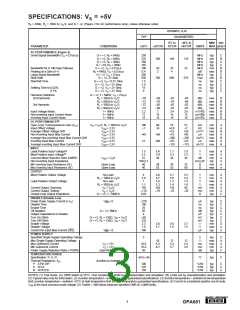
Bandwidth for 0.1dB Gain Flatness
Peaking at a Gain of +1
Large Signal Bandwidth
Slew Rate
50
2
45
4
min
max
typ
min
typ
typ
typ
typ
1600
1600
1200
Rise/Fall Time
ns
ns
ns
Settling Time to 0.02%
0.1%
8
Harmonic Distortion
2nd Harmonic
G = +2, f = 5MHz, VO = 2Vp-p
RL = 100Ω
–79
–85
–74
–77
2.5
12
15
0.001
0.008
0.01
0.05
–73
–77
–71
–75
3.0
14
–70
–70
–71
–74
3.4
15
–68
–69
–68
–72
3.6
15
dBc
dBc
dBc
max
max
max
max
max
max
max
typ
B
B
B
B
B
B
B
C
C
C
C
R
L ≥ 500Ω
RL = 100Ω
L ≥ 500Ω
3rd Harmonic
R
dBc
Input Voltage Noise
f > 1MHz
f > 1MHz
f > 1MHz
nV/√Hz
pA/√Hz
pA/√Hz
%
%
deg
Non-Inverting Input Current Noise
Inverting Input Current Noise
Differential Gain
18
18
19
G = +2, NTSC, VO = 1.4Vp, RL = 150Ω
RL = 37.5Ω
G = +2, NTSC, VO = 1.4Vp, RL = 150Ω
RL = 37.5Ω
typ
typ
typ
Differential Phase
deg
DC PERFORMANCE(4)
Open-Loop Transimpedance Gain (ZOL
Input Offset Voltage
Average Offset Voltage Drift
Non-Inverting Input Bias Current
Average Non-Inverting Input Bias Current Drift
Inverting Input Bias Current
)
VO = 0V, RL = 100Ω
VCM = 0V
100
±1.3
56
±5
56
±6.5
+35
±65
–400
±50
56
±7.5
+40
±85
–450
±55
kΩ
mV
µV/°C
µA
nA/°C
µA
nA°/C
min
max
max
max
max
max
max
A
A
B
A
B
A
B
VCM = 0V
VCM = 0V
+30
+55
VCM = 0V
VCM = 0V
VCM = 0V
±10
±40
Average Inverting Input Bias Current Drift
–125
–150
INPUT
Common-Mode Input Range(5)
Common-Mode Rejection
Non-Inverting Input Impedance
Min Inverting Input Resistance (RI)
Max Inverting Input Resistance (RI)
±3.5
52
100 || 2
41
±3.4
±3.3
46
±3.2
45
V
dB
kΩ || pF
Ω
min
min
typ
min
max
A
A
C
A
A
VCM = 0V
47
Open-Loop
Open-Loop
33
48
31
50
30
55
41
Ω
OUTPUT™
Voltage Output Swing
No Load
100Ω Load
VO = 0
±4.0
±3.9
+190
–150
0.03
±3.8
±3.7
+160
–135
±3.7
±3.6
+140
–130
±3.6
±3.3
+80
–80
V
V
mA
mA
Ω
min
min
min
min
typ
A
A
A
A
C
Current Output, Sourcing
Current Output, Sinking
Closed-Loop Output Impedance
VO = 0
G = +2, f = 100kHz
DISABLE (Disabled Low)
Power Down Supply Current (+VS)
Disable Time
Enable Time
Off Isolation
Output Capacitance in Disable
Turn On Glitch
Turn Off Glitch
Enable Voltage
Disable Voltage
VDIS = 0
–320
100
25
70
4
±50
±20
3.3
1.8
100
µA
ns
ns
dB
pF
mV
mV
V
typ
typ
typ
typ
typ
typ
typ
min
max
max
C
C
C
C
C
C
C
A
A
A
G = +2, 5MHz
G = +2, RL = 150Ω, VIN = 0
G = +2, RL = 150Ω, VIN = 0
3.5
1.7
160
3.6
1.6
160
3.7
1.5
160
V
µA
Control Pin Input Bias Current (DIS)
V
DIS = 0
POWER SUPPLY
Specified Operating Voltage
Maximum Operating Voltage Range
Max Quiescent Current
Min Quiescent Current
Power Supply Rejection Ratio (–PSRR)
±5
V
V
mA
mA
dB
typ
max
max
min
min
C
A
A
A
A
±6
6.4
5.6
52
±6
6.5
5.5
50
±6
6.6
5.0
49
VS = ±5V
S = ±5V
Input Referred
6
6
58
V
TEMPERATURE RANGE
Specification: P, U, N
–40 to +85
°C
typ
C
Thermal Resistance, θJA
Junction-to-Ambient
P
U
N
8-Pin DIP
SO-8
SOT23-6
100
125
150
°C/W
°C/W
°C/W
typ
typ
typ
C
C
C
NOTES: (1) Test levels: (A) 100% tested at 25°C. Over temperature limits by characterization and simulation. (B) Limits set by characterization and simulation.
(C) Typical value only for information. (2) Junction temperature = ambient for 25°C guaranteed specifications. (3) Junction temperature = ambient at low temperature
limit: junction temperature = ambient +23°C at high temperature limit for over temperature guaranteed specifications. (4) Current is considered positive out-of-node.
VCM is the input common-mode voltage. (5) Tested < 3dB below minimum specified CMR at ± CMIR limits.
®
2
OPA681

 BB [ BURR-BROWN CORPORATION ]