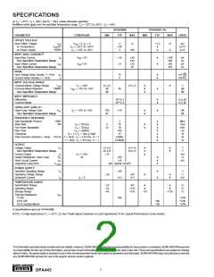
SPECIFICATIONS
At TA = +25°C, VS = ±40V, and RL = 5kΩ, unless otherwise specified.
Boldface limits apply over the specified temperature range, TA = –25°C to +85°C. VS = ±40V.
OPA445BM
OPA445AP, AU
TYP
PARAMETER
CONDITIONS
MIN
TYP
MAX
MIN
MAX
UNITS
OFFSET VOLTAGE
Input Offset Voltage
vs Temperature
VOS
VOS/dT
PSRR
VCM = 0, IO = 0
TA = –25°C to +85°C
VS = ±10V to ±45V
±1
±10
4
±3
±1.5
✻
✻
±5
mV
µV/°C
µV/V
vs Power Supply
100
✻
INPUT BIAS CURRENT(1)
Input Bias Current
Over Specified Temperature Range
Input Offset Current
IB
VCM = 0V
VCM = 0V
±10
±4
±50
±10
±20
±5
✻
✻
±100
±20
±40
±10
pA
nA
pA
nA
IOS
Over Specified Temperature Range
NOISE
Input Voltage Noise Density, f = 1kHz
Current Noise Density, f = 1kHz
en
in
15
6
✻
✻
nV/√Hz
fA/√Hz
INPUT VOLTAGE RANGE
Common-Mode Voltage Range
Common-Mode Rejection
Over Specified Temperature Range
VCM
CMRR
VS = ±40V
VCM = –35V to +35V
(V–)+5
80
80
(V+)–5
✻
✻
✻
✻
V
dB
dB
95
✻
INPUT IMPEDANCE
Differential
Common-Mode
1013 || 1
1014 || 3
✻
✻
Ω || pF
Ω || pF
OPEN-LOOP GAIN, DC
Open-Loop Voltage Gain
Over Specified Temperature Range
AOL
VO = –35V to +35V
100
97
110
✻
✻
✻
dB
dB
FREQUENCY RESPONSE
Gain Bandwidth Product
Slew Rate
Full Power Bandwidth
Rise Time
GBW
SR
2
15
70
100
35
✻
✻
✻
✻
✻
✻
✻
MHz
V/µs
kHz
ns
%
%
VO = 70Vp-p
VO = 70Vp-p
VO = ±200mV
5
23
✻
✻
Overshoot
G = +1, ZL = 5kΩ || 50pF
f = 1kHz, VO = 3.5Vrms, G = 1
f = 1kHz, VO = 10Vrms, G = 1
Total Harmonic Distortion + Noise THD+N
0.0002
0.00008
%
OUTPUT
Voltage Output
Over Specified Temperature Range
Current Output
Output Resistance, Open Loop
Short Circuit Current
Capacitive Load Drive
VO
(V–)+5
(V–)+5
±15
(V+)–5
(V+)–5
✻
✻
✻
✻
✻
V
V
mA
Ω
IO
RO
ISC
VO = ±28V
dc
220
±26
✻
✻
✻
mA
CLOAD
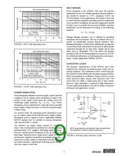
See Typical Curve(2)
POWER SUPPLY
Specified Operating Range
Operating Voltage Range
Quiescent Current
VS
IQ
±40
✻
✻
V
V
mA
±10
±45
±4.7
✻
✻
✻
IO = 0
±4.2
TEMPERATURE RANGE
Specification Range
Operating Range
Storage Range
–25
–55
–65
+85
+125
+125
✻
✻
–55
✻
✻
+125
°C
°C
°C
Thermal Resistance
TO-99
8-Pin DIP
θJA
200
°C/W
°C/W
°C/W
100
150
SO-8 Surface-Mount
✻ Specifications same as OPA445BM.
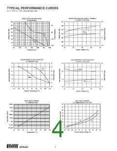
NOTE: (1) High-speed test at TJ = +25°C. (2) See “Small-Signal Overshoot vs Load Capacitance” in the Typical Performance Curves section.
The information provided herein is believed to be reliable; however, BURR-BROWN assumes no responsibility for inaccuracies or omissions. BURR-BROWN assumes
no responsibility for the use of this information, and all use of such information shall be entirely at the user’s own risk. Prices and specifications are subject to change
without notice. No patent rights or licenses to any of the circuits described herein are implied or granted to any third party. BURR-BROWN does not authorize or warrant
any BURR-BROWN product for use in life support devices and/or systems.
®
2
OPA445

 BB [ BURR-BROWN CORPORATION ]