BIAS CURRENT CHANGE
APPLICATIONS CIRCUITS
vs COMMON-MODE VOLTAGE
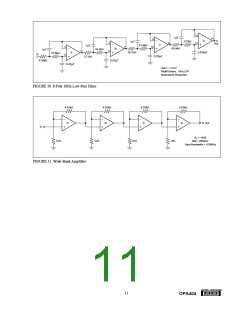
Figures 5 through 11 are circuit diagrams of various appli-
cations for the OPA404.
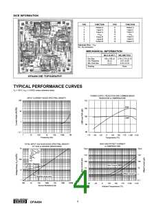
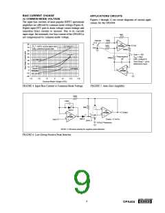
The input bias currents of most popular BIFET operational
amplifiers are affected by common-mode voltage (Figure 4).
Higher input FET gate-to-drain voltage causes leakage and
ionization (bias) currents to increase. Due to its cascode
input stage, the extremely low bias current of the OPA404 is
not compromised by common-mode voltage.
1MΩ
10kΩ
100Ω
Operate
2
3
1/4
OPA404
80
1
In
Zero
Out
LF156/157
TA = +25°C; curves taken from
mfg. published typical data
70
60
50
100kΩ
AD547
Gain = –100
Polypropylene
1µF
VOS < 10µV
40
30
LF155
100kΩ
Drift ≈ 0.05µV/°C
Zero Droop ≈ 1µV/s
Referred to Input
LF156/157
20
LF155
AD547
OPA404
6
10
OPA404
1/4
OPA404
7
0
5
–10
–20
OP-15/16/17
–15
–10
–5
0
+5
+10
+15
Common-Mode Voltage (VDC)
FIGURE 4. Input Bias Current vs Common-Mode Voltage.
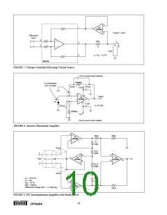
FIGURE 5. Auto-Zero Amplifier.
10kΩ
≈10pF
(1)
1MΩ
6
IN914
1/4
OPA404
7
Output
2
3
(1)
5
(1)
1/4
OPA404
1
IN914
Input
Droop ≈ 0.1mV/s
0.01µF Polstyrene
2N4117
NOTE: (1) Reverse polarity for negative peak detection.
FIGURE 6. Low-Droop Positive Peak Detector.
®
9
OPA404

 BB [ BURR-BROWN CORPORATION ]