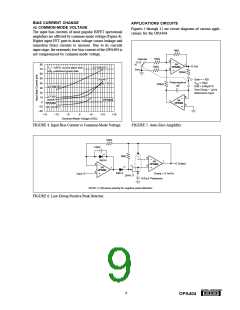
GUARDING AND SHIELDING
APPLICATIONS INFORMATION
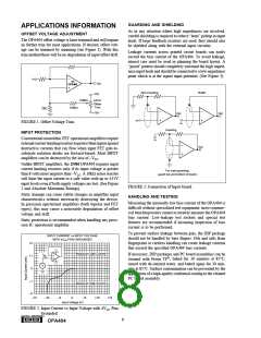
OFFSET VOLTAGE ADJUSTMENT
As in any situation where high impedances are involved,
careful shielding is required to reduce “hum” pickup in input
leads. If large feedback resistors are used, they should also
be shielded along with the external input circuitry.
The OPA404 offset voltage is laser-trimmed and will require
no further trim for most applications. If desired, offset volt-
age can be trimmed by summing (see Figure 1). With this
trim method there will be no degradation of input offset drift.
Leakage currents across printed circuit boards can easily
exceed the bias current of the OPA404. To avoid leakage,
utmost care must be used in planning the board layout. A
“guard” pattern should completely surround the high imped-
ance input leads and should be connected to a low-impedance
point which is at the signal input potential. (See Figure 3).
In
1/4
Out
OPA404
Non-Inverting
Buffer
–15V
100kΩ
±2mV
Offset
Trim
150kΩ
20Ω
+15V
Out
Out
In
FIGURE 1. Offset Voltage Trim.
In
Inverting
INPUT PROTECTION
Conventional monolithic FET operational amplifiers require
externalcurrent-limitingresistorstoprotecttheirinputsagainst
destructive currents that can flow when input FET gate-to-
substrate isolation diodes are forward-biased. Most BIFET
In
Out
amplifiers can be destroyed by the loss of –VCC
.
Unlike BIFET amplifiers, the Difet OPA404 requires input
current limiting resistors only if its input voltage is greater
than 8 volts more negative than –VCC. A 10kΩ series resistor
will limit the input current to a safe value with up to ±15V
input levels even if both supply voltages are lost. (See Figure
2 and Absolute Maximum Ratings).
For input guarding,
guard top and bottom of board.
FIGURE 3. Connection of Input Guard.
Static damage can cause subtle changes in amplifier input
characteristics without necessarily destroying the device.
In precision operational amplifiers (both bipolar and FET
types), this may cause a noticeable degradation of offset
voltage and drift.
HANDLING AND TESTING
Measuring the unusually low bias current of the OPA404 is
difficult without specialized test equipment; most commer-
cial benchtop testers cannot accurately measure the OPA404
bias current. Low-leakage test sockets and special test
fixtures are recommended if incoming inspection of bias
current is to be performed.
Static protection is recommended when handling any preci-
sion IC operational amplifier.
To prevent surface leakage between pins, the DIP package
should not be handled by bare fingers. Oils and salts from
fingerprints or careless handling can create leakage currents
that exceed the specified OPA404 bias currents.
INPUT CURRENT vs INPUT VOLTAGE
WITH ±VCC PINS GROUNDED
+2
Maximum Safe Current
If necessary, DIP packages and PC board assemblies can be
cleaned with Freon TF®, baked for 30 minutes at 85°C,
rinsed with de-ionized water, and baked again for 30 min-
utes at 85°C. Surface contamination can be prevented by the
application of a high-quality conformal coating to the cleaned
PC board assembly.
IIN
+1
V
0
–1
Maximum Safe Current
–2
–15
–10
–5
0
+5
+10
+15
Input Voltage (V)
FIGURE 2. Input Current vs Input Voltage with ±VCC Pins
Grounded.
®
8
OPA404

 BB [ BURR-BROWN CORPORATION ]