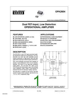
SPECIFICATIONS
ELECTRICAL
At TA = +25°C, VS = ±15V, unless otherwise noted.
OPA2604AP, AU
TYP
PARAMETER
CONDITION
MIN
MAX
UNITS
OFFSET VOLTAGE
Input Offset Voltage
Average Drift
±1
±8
80
±5
mV
µV/°C
dB
Power Supply Rejection
VS = ±5 to ±24V
70
INPUT BIAS CURRENT(1)
Input Bias Current
Input Offset Current
VCM = 0V
VCM = 0V
100
±4
pA
pA
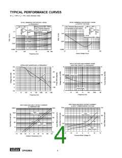
NOISE
Input Voltage Noise
Noise Density: f = 10Hz
f = 100Hz
25
15
11
10
1.5
nV/√Hz
nV/√Hz
nV/√Hz
nV/√Hz
µVp-p
f = 1kHz
f = 10kHz
Voltage Noise, BW = 20Hz to 20kHz
Input Bias Current Noise
Current Noise Density, f = 0.1Hz to 20kHz
6
fA/√Hz
INPUT VOLTAGE RANGE
Common-Mode Input Range
Common-Mode Rejection
±12
80
±13
100
V
dB
VCM = ±12V
INPUT IMPEDANCE
Differential
Common-Mode
1012 || 8
1012 || 10
Ω || pF
Ω || pF
OPEN-LOOP GAIN
Open-Loop Voltage Gain
VO = ±10V, RL = 1kΩ
80
15
100
dB
FREQUENCY RESPONSE
Gain-Bandwidth Product
Slew Rate
Settling Time: 0.01%
0.1%
G = 100
20Vp-p, RL = 1kΩ
G = –1, 10V Step
20
25
1.5
MHz
V/µs
µs
1
µs
Total Harmonic Distortion + Noise (THD+N)
G = 1, f = 1kHz
VO = 3.5Vrms, RL = 1kΩ
f = 1kHz, RL = 1kΩ
0.0003
%
Channel Separation
142
dB
OUTPUT
Voltage Output
Current Output
Short Circuit Current
Output Resistance, Open-Loop
RL = 600Ω
VO = ±12V
±11
±12
±35
±40
25
V
mA
mA
Ω
POWER SUPPLY
Specified Operating Voltage
Operating Voltage Range
Current, Total Both Amplifiers
±15
V
V
mA
±4.5
±24
±12
IO = 0
±10.5
TEMPERATURE RANGE
Specification
Storage
Thermal Resistance(2), θJA
–25
–40
+85
+125
°C
°C
°C/W
90
NOTES: (1) Typical performance, measured fully warmed-up. (2) Soldered to circuit board—see text.
The information provided herein is believed to be reliable; however, BURR-BROWN assumes no responsibility for inaccuracies or omissions. BURR-BROWN assumes
no responsibility for the use of this information, and all use of such information shall be entirely at the user’s own risk. Prices and specifications are subject to change
without notice. No patent rights or licenses to any of the circuits described herein are implied or granted to any third party. BURR-BROWN does not authorize or warrant
any BURR-BROWN product for use in life support devices and/or systems.
®
OPA2604
2

 BB [ BURR-BROWN CORPORATION ]