APPLICATIONS INFORMATION
The OPA2604 is unity-gain stable, making it easy to use in a
wide range of circuitry. Applications with noisy or high
impedance power supply lines may require decoupling ca-
pacitors close to the device pins. In most cases 1µF tantalum
capacitors are adequate.
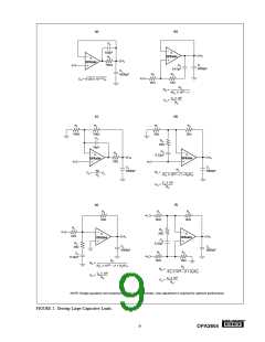
and capacitive load will decrease the phase margin and may
lead to gain peaking or oscillations. Load capacitance reacts
with the op amp’s open-loop output resistance to form an
additional pole in the feedback loop. Figure 2 shows various
circuits which preserve phase margin with capacitive load.
Request Application Bulletin AB-028 for details of analysis
techniques and applications circuits.
DISTORTION MEASUREMENTS
For the unity-gain buffer, Figure 2a, stability is preserved by
adding a phase-lead network, RC and CC. Voltage drop across
RC will reduce output voltage swing with heavy loads. An
alternate circuit, Figure 2b, does not limit the output with low
load impedance. It provides a small amount of positive feed-
backtoreducethenetfeedbackfactor.Inputimpedanceofthis
circuit falls at high frequency as op amp gain rolloff reduces
the bootstrap action on the compensation network.
The distortion produced by the OPA2604 is below the mea-
surement limit of virtually all commercially available equip-
ment. Aspecialtestcircuit, however, canbeusedtoextendthe
measurement capabilities.
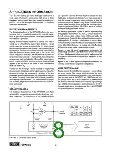
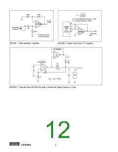
Op amp distortion can be considered an internal error source
which can be referred to the input. Figure 1 shows a circuit
which causes the op amp distortion to be 101 times greater
than normally produced by the op amp. The addition of R3 to
the otherwise standard non-inverting amplifier configuration
alters the feedback factor or noise gain of the circuit. The
closed-loop gain is unchanged, but the feedback available for
error correction is reduced by a factor of 101. This extends the
measurement limit, including the effects of the signal-source
purity, by a factor of 101. Note that the input signal and load
applied to the op amp are the same as with conventional
feedback without R3.
Figures 2c and 2d show compensation techniques for
noninverting amplifiers. Like the follower circuits, the circuit
in Figure 2d eliminates voltage drop due to load current, but
at the penalty of somewhat reduced input impedance at high
frequency.
Figures 2e and 2f show input lead compensation networks for
inverting and difference amplifier configurations.
NOISE PERFORMANCE
Validity of this technique can be verified by duplicating
measurements at high gain and/or high frequency where the
distortion is within the measurement capability of the test
equipment. Measurements for this data sheet were made with
the Audio Precision System One which greatly simplifies
such repetitive measurements. The measurement technique
can, however, be performed with manual distortion measure-
ment instruments.
Op amp noise is described by two parameters—noise voltage
and noise current. The voltage noise determines the noise
performance with low source impedance. Low noise bipolar-
input op amps such as the OPA27 and OPA37 provide very
low voltage noise. But if source impedance is greater than a
fewthousandohms,thecurrentnoiseofbipolar-inputopamps
react with the source impedance and will dominate. At a few
thousand ohms source impedance and above, the OPA2604
will generally provide lower noise.
CAPACITIVE LOADS
The dynamic characteristics of the OPA2604 have been
optimized for commonly encountered gains, loads and oper-
ating conditions. The combination of low closed-loop gain
R1
R2
SIG. DIST.
R1
R2
R3
GAIN GAIN
1
1
101
∞
5kΩ
50Ω
2
R3
VO = 10Vp-p
(3.5Vrms)
OPA2604
10
101 500Ω 5kΩ 500Ω
100
101
50Ω
5kΩ
∞
Generator
Output
Analyzer
Input
RL
1kΩ
Audio Precision
System One
Analyzer*
IBM PC
or
Compatible
* Measurement BW = 80kHz
FIGURE 1. Distortion Test Circuit.
®
OPA2604
8

 BB [ BURR-BROWN CORPORATION ]