CIRCUIT BOARD LAYOUT
1000MΩ
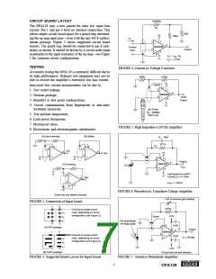
The OPA129 uses a new pinout for ultra low input bias
current. Pin 1 and pin 4 have no internal connection. This
allows ample circuit board space for a guard ring surround-
ing the op amp input pins—even with the tiny SO-8 surface-
mount package. Figure 3 shows suggested circuit board
layouts. The guard ring should be connected to pin 8 (sub-
strate) as shown. It should be driven by a circuit node equal
in potential to the input terminals of the op amp—see Figure
2 for common circuit configurations.
RF
2kΩ
V+
18kΩ
IIN
2
7
6
OPA129
Current
Input
3
Output
5
8
VO = –IIN • RF
VO = –1V/nA
V–
TESTING
FIGURE 4. Current-to-Voltage Converter.
Accurately testing the OPA129 is extremely difficult due to
its high performance. Ordinary test equipment may not be
able to resolve the amplifier’s extremely low bias current.
500Ω
9.5kΩ
V+
8
Guard
2
Inaccurate bias current measurements can be due to:
1. Test socket leakage,
7
6
OPA129
2. Unclean package,
3
1VDC
Output
5
3. Humidity or dew point condensations,
4. Circuit contamination from fingerprints or anti-static
treatment chemicals,
V–
pH Probe
S ≈ 500MΩ
50mV Out
R
5. Test ambient temperature,
6. Load power dissipation,
7. Mechanical stress,
FIGURE 5. High Impedance (1015Ω) Amplifier.
8. Electrostatic and electromagnetic interference.
(A) Non-Inverting
(B) Buffer
CF 10pF
1011Ω
RF
8
2
8
2
3
Out
6
6
V+
8
Out
3
In
In
2
3
7
Output
VOUT
6
OPA129
(C) Inverting
∆Q
5
Low frequency cutoff =
1/(2πRFCF) = 0.16Hz
In
2
V–
Out
6
3
VOUT = –∆Q/CF
8
FIGURE 6. Piezoelectric Transducer Charge Amplifier.
Guard top and bottom of board.
~1pF to prevent gain peaking
FIGURE 2. Connection of Input Guard.
1
8
1010
Ω
Connect to proper circuit
node, depending on circuit
configuration (see Figure 2).
V+
V0
+15V
Guard
Pin photodiode
HP 5082-4204
V–
4
5
8
0.1µF
2
3
(A) DIP package
7
Output
6
1
8
OPA129
Connect to proper circuit
node, depending on circuit
configuration (see Figure 2).
0.1µF
5
5 x 10⁹V/W
V+
V0
V–
4
–15V
Circuit must be well shielded.
5
(B) SOIC package
FIGURE 3. Suggested Board Layout for Input Guard.
FIGURE 7. Sensitive Photodiode Amplifier.
®
7
OPA129

 BB [ BURR-BROWN CORPORATION ]