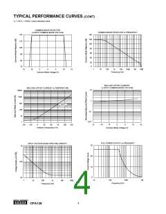
TYPICAL PERFORMANCE CURVES (CONT)
TA = +25°C, +15VDC, unless otherwise noted.
COMMON-MODE INPUT RANGE vs SUPPLY VOLTAGE
BIAS CURRENT vs ADDITIONAL POWER DISSIPATION
15
10
100pA
10pA
1pA
100
5
0
10
1
0
5
10
15
20
0
50
100
150
200
250
300
350
Additional Power Dissipation (mW)
Supply Voltage (±VCC
)
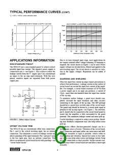
Due to its laser-trimmed input stage, most applications do
not require external offset voltage trimming. If trimming is
required, the circuit shown in Figure 1 can be used. Power
supply voltages are divided down, filtered and applied to the
non-inverting input. The circuit shown is sensitive to varia-
tion in the supply voltages. Regulation can be added, if
needed.
APPLICATIONS INFORMATION
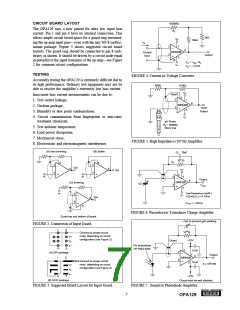
NON-STANDARD PINOUT
The OPA129 uses a non-standard pinout to achieve lowest
possible input bias current. The negative power supply is
connected to pin 5—see Figure 1. This is done to reduce the
leakage current from the V- supply (pin 4 on conventional
op amps) to the op amp input terminals. With this new
pinout, sensitive inputs are separated from both power
supply pins.
GUARDING AND SHIELDING
Ultra-low input bias current op amps require precautions to
achieve best performance. Leakage current on the surface of
circuit board can exceed the input bias current of the ampli-
fier. For example, a circuit board resistance of 1012Ω from
a power supply pin to an input pin produces a current of
15pA—more than one-hundred times the input bias current
of the op amp.
RF
V+
RIN
2
VIN
7
6
VOUT
OPA129
To minimize surface leakage, a guard trace should com-
pletely surround the input terminals and other circuitry
connecting to the inputs of the op amp. The DIP package
should have a guard trace on both sides of the circuit board.
The guard ring should be driven by a circuit node equal in
potential to the op amp inputs—see Figure 2. The substrate,
pin 8, should also be connected to the circuit board guard to
assure that the amplifier is fully surrounded by the guard
potential. This minimizes leakage current and noise pick-up.
3
5
V+
V–
V–
470kΩ
470kΩ
220Ω
0.1µF
Careful shielding is required to reduce noise pickup. Shield-
ing near feedback components may also help reduce noise
pick-up.
FIGURE 1. Offset Adjust Circuit.
OFFSET VOLTAGE TRIM
Triboelectric effects (friction-generated charge) can be a
troublesome source of errors. Vibration of the circuit board,
input connectors and input cables can cause noise and drift.
Make the assembly as rigid as possible. Attach cables to
avoid motion and vibration. Special low noise or low leak-
age cables may help reduce noise and leakage current. Keep
all input connections as short possible. Surface-mount com-
ponents may reduce circuit board size and allow a more rigid
assembly.
The OPA129 has no conventional offset trim connections.
Pin 1, next to the critical inverting input, has no internal
connection. This eliminates a source of leakage current and
allows guarding of the input terminals. Pin 1 and pin 4, next
to the two input pins, have no internal connection. This
allows an optimized circuit board layout with guarding—see
“circuit board layout.”
®
6
OPA129

 BB [ BURR-BROWN CORPORATION ]