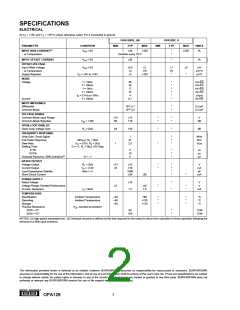
SPECIFICATIONS
ELECTRICAL
At VS = ±15V and TA = +25°C unless otherwise noted. Pin 8 connected to ground.
OPA129PB, UB
TYP
OPA129P, U
TYP
PARAMETER
CONDITION
MIN
MAX
MIN
MAX
UNITS
INPUT BIAS CURRENT(1)
vs Temperature
VCM = 0V
±30
±100
*
*
±250
fA
Doubles every 10°C
INPUT OFFSET CURRENT
V
V
CM = 0V
CM = 0V
±30
*
fA
OFFSET VOLTAGE
Input Offset Voltage
vs Temperature
±0.5
±3
±3
±2
±10
±100
±1
±5
*
±5
mV
µV/°C
µV/V
Supply Rejection
V
S = ±5V to ±18V
*
NOISE
Voltage
f = 10Hz
f = 100Hz
f = 1kHz
85
28
17
15
4
*
*
*
*
*
*
nV/√Hz
nV/√Hz
nV/√Hz
nV/√Hz
µVp-p
f = 10kHz
f
B = 0.1Hz to 10Hz
Current
f = 10kHz
0.1
fA/√Hz
INPUT IMPEDANCE
Differential
Common-Mode
1013 || 1
1015 || 2
*
*
Ω || pF
Ω || pF
VOLTAGE RANGE
Common-Mode Input Range
Common-Mode Rejection
±10
80
±12
118
*
*
*
*
V
dB
V
IN = ±10V
L ≥ 2kΩ
OPEN-LOOP GAIN, DC
Open-Loop Voltage Gain
R
94
1
120
*
*
dB
FREQUENCY RESPONSE
Unity Gain, Small Signal
Full Power Response
Slew Rate
1
47
2.5
*
*
*
MHz
kHz
V/µs
20Vp-p, RL = 2kΩ
O = ±10V, RL = 2kΩ
V
*
Settling Time:
G = –1, RL = 2kΩ, 10V Step
0.1%
0.01%
5
10
5
*
*
*
µs
µs
µs
Overload Recovery, 50% Overdrive(2)
G = –1
RATED OUTPUT
Voltage Output
Current Output
Load Capacitance Stability
Short-Circuit Current
R
V
L = 2kΩ
O = ±12V
Gain = +1
±12
±6
±13
±10
1000
±35
*
*
*
*
*
*
V
mA
pF
±55
*
mA
POWER SUPPLY
Rated Voltage
Voltage Range, Derated Performance
Current, Quiescent
±15
*
*
V
V
mA
±5
±18
1.8
*
*
*
I
O = 0mA
1.2
TEMPERATURE
Specification
Operating
Ambient Temperature
Ambient Temperature
–40
–40
–40
+85
+125
+125
*
*
*
*
*
*
°C
°C
°C
Storage
Thermal Resistance
PDIP—"P"
θJA, Junction-to-Ambient
90
100
*
*
°C/W
°C/W
SOIC—"U"
NOTES: (1) High-speed automated test. (2) Overload recovery is defined as the time required for the output to return from saturation to linear operation following the
removal of a 50% input overdrive.
The information provided herein is believed to be reliable; however, BURR-BROWN assumes no responsibility for inaccuracies or omissions. BURR-BROWN
assumes no responsibility for the use of this information, and all use of such information shall be entirely at the user’s own risk. Prices and specifications are subject
to change without notice. No patent rights or licenses to any of the circuits described herein are implied or granted to any third party. BURR-BROWN does not
authorize or warrant any BURR-BROWN product for use in life support devices and/or systems.
®
2
OPA129

 BB [ BURR-BROWN CORPORATION ]