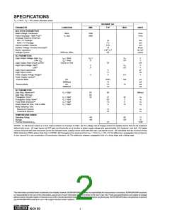
ABSOLUTE MAXIMUM RATINGS
PACKAGE INFORMATION(1)
PACKAGE DRAWING
NUMBER
Storage Temperature ......................................................... –40°C to +125°C
Supply Voltages, VS ...................................................................... –0.5 to 6V
Transmitter Input Voltage, VI ............................................. –0.5 to VS + 0.5V
Receiver Output Voltage, VO ............................................. –0.5 to VS + 0.5V
R/TX Inputs......................................................................... –0.5 to VS + 0.5V
Isolation Voltage dV/dt, VISO ............................................................ 500kV/µs
MODEL
PACKAGE
ISO150AP
ISO150AU
24-Pin Single-Wide DIP
28-Lead SOIC
243-1
217-2
NOTE: (1) For detailed drawing and dimension table, please see end of
data sheet, or Appendix D of Burr-Brown IC Data Book.
D
X Short to Ground ...................................................................... Continuous
Junction Temperature, TJ .................................................................... 175°C
Lead Temperature (soldering, 10s) ..................................................... 260°C
1.6mm below seating plane (DIP package) ......................................... 300°C
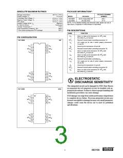
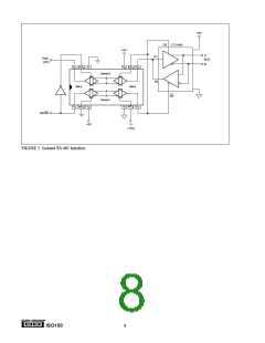
PIN DESCRIPTIONS
NAME
FUNCTION
D1A
Data in or data out for transceiver 1A. R/T1A held
low makes D1A an input pin.
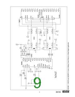
PIN CONFIGURATION
R/T1A
VSA
Receive/Transmit switch controlling transceiver 1A.
TOP VIEW
DIP
+5V supply pin for side A which powers transceivers
1A and 2A.
D1A
R/T1A
VSA
1
2
3
24 D2A
23 R/T2A
22 GA
GB
R/T1B
D1B
Ground pin for transceivers 1B and 2B.
Receive/Transmit switch controlling transceiver 1B.
Data in or data out for transceiver 1B. R/T1B held
low makes D1B an input pin.
D2B
Data in or data out for transceiver 2B. R/T2B held
low makes D2B an input pin.
R/T2B
VSB
Receive/Transmit switch controlling D2B.
+5V supply pin for side B which powers transceivers
1B and 2B.
GA
R/T2A
D2A
Ground pin for transceivers 1A and 2A.
Receive/Transmit switch controlling transceiver 2A.
Data in or data out for transceiver 2A. R/T2A held
low makes D2A in input pin.
GB 10
R/T1B 11
D1B 12
15 VSB
14 R/T2B
13 D2B
ELECTROSTATIC
DISCHARGE SENSITIVITY
This integrated circuit can be damaged by ESD. Burr-Brown
recommends that all integrated circuits be handled with ap-
propriate precautions. Failure to observe proper handling and
installation procedures can cause damage.
TOP VIEW
SOIC
ESD damage can range from subtle performance degradation
to complete device failure. Precision integrated circuits may
be more susceptible to damage because very small parametric
changes could cause the device not to meet its published
specifications.
D1A
R/T1A
VSA
1
2
3
28 D2A
27 R/T2A
26 GA
GB 12
R/T1B 13
D1B 14
17 VSB
16 R/T2B
15 D2B
®
3
ISO150

 BB [ BURR-BROWN CORPORATION ]