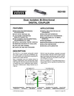
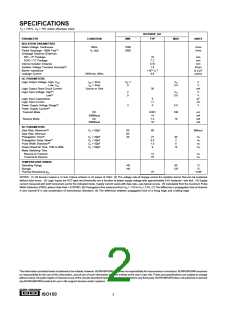
SPECIFICATIONS
TA = +25°C, VS = +5V unless otherwise noted.
ISO150AP, AU
TYP
PARAMETER
CONDITION
MIN
MAX
UNITS
ISOLATION PARAMETERS
Rated Voltage, Continuous
Partial Discharge, 100% Test(1)
Creepage Distance (External)
DIP—“P” Package
60Hz
1s, 5pC
1500
2400
Vrms
Vrms
16
7.2
mm
mm
SOIC—“U” Package
Internal Isolation Distance
Isolation Voltage Transient Immunity(2)
Barrier Impedance
0.10
1.6
>1014 || 7
0.6
mm
kV/µs
Ω || pF
µArms
Leakage Current
240Vrms, 60Hz
DC PARAMETERS
Logic Output Voltage, High, VOH
Low, VOL
IOH = 6mA
IOL = 6mA
VS–1
0
VS
0.4
V
V
Logic Output Short-Circuit Current
Logic Input Voltage, High(3)
Low(3)
Source or Sink
30
mA
V
V
2
0
VS
0.8
Logic Input Capacitance
Logic Input Current
Power Supply Voltage Range(3)
Power Supply Current(4)
Transmit Mode
5
<1
5
pF
nA
V
3
5.5
100
10
DC
50MBaud
DC
0.001
14
7.2
16
µA
mA
mA
mA
Receive Mode
50MBaud
AC PARAMETERS
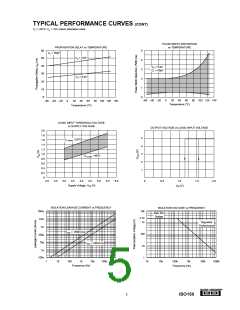
Data Rate, Maximum(5)
Data Rate, Minimum
CL = 50pF
50
DC
20
80
MBaud
Propagation Time(6)
CL = 50pF
CL = 50pF
CL = 50pF
27
0.5
1.5
9
40
2
6
ns
ns
ns
ns
Propagation Delay Skew(7)
Pulse Width Distortion(8)
Output Rise/Fall Time, 10% to 90%
Mode Switching Time
Receive-to-Transmit
C
L = 50pF
14
13
75
ns
ns
Transmit-to-Receive
TEMPERATURE RANGE
Operating Range
Storage
–40
–40
85
125
°C
°C
Thermal Resistance,θJA
75
°C/W
NOTES: (1) All devices receive a 1s test. Failure criterion is ≥5 pulses of ≥5pC. (2) The voltage rate-of-change across the isolation barrier that can be sustained
without data errors. (3) Logic inputs are HCT-type and thresholds are a function of power supply voltage with approximately 0.4V hystersis—see text. (4) Supply
current measured with both tranceivers set for the indicated mode. Supply current varies with data rate—see typical curves. (5) Calculated from the maximum Pulse
Width Distortion (PWD), where Data Rate = 0.3/PWD. (6) Propagation time measured from VIN = 1.5V to VO = 2.5V. (7) The difference in propagation time of channel
A and channel B in any combination of transmission directions. (8) The difference between progagation time of a rising edge and a falling edge.
The information provided herein is believed to be reliable; however, BURR-BROWN assumes no responsibility for inaccuracies or omissions. BURR-BROWN assumes
no responsibility for the use of this information, and all use of such information shall be entirely at the user’s own risk. Prices and specifications are subject to change
without notice. No patent rights or licenses to any of the circuits described herein are implied or granted to any third party. BURR-BROWN does not authorize or warrant
any BURR-BROWN product for use in life support devices and/or systems.
®
ISO150
2

 BB [ BURR-BROWN CORPORATION ]