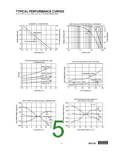
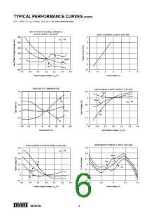
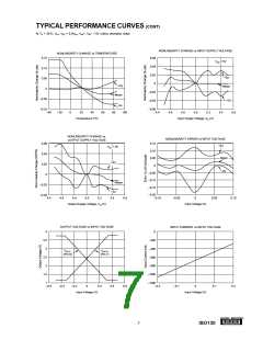
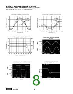
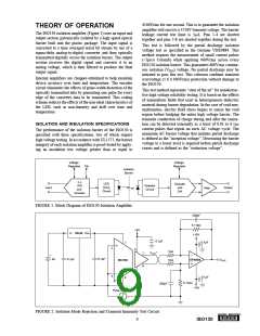
SPECIFICATIONS
At VIN+, VIN– = 0V, TA = 25°C, VS1, VS2 = 5.0V unless otherwise noted.
ISO130P/ISO130PB
ISO130U/ISO130UB
PARAMETER
CONDITIONS
MIN
TYP
MAX
UNITS
INPUT
Initial Offset Voltage
vs Temperature
vs VS1
–1.8
–0.9
4.6
30
0.0
mV
µV/°C
µV/V
µV/V
vs VS2
–40
Power Supply Rejection; VS1
and VS2 Together
Noise
1MHz Square Wave, 5ns Rise/Fall Time
0.1Hz to 100kHz
5
300
mV/V
µVrms
mV
Input Voltage Range
–200
200
Maximum Input Voltage Range before Output Clipping
Initial Input Bias Current(3)
vs Temperature
±300
–670
3
530
0.38
72
mV
nA
nA/°C
kΩ
%/°C
dB
Input Resistance(3)
vs Temperature
Common-Mode Rejection Ratio(4)
GAIN(5)
Initial Gain
ISO130P/ISO130U
ISO130PB/ISO130UB
Gain vs Temperature
Gain vs VS1
–200mV < VIN+ < 200mV
–200mV < VIN+ < 200mV
7.61
7.85
8.00
7.93
10
2.1
–0.6
8.40
8.01
V/V
V/V
ppm/°C
ppm/mV
ppm/mV
Gain vs VS2
Gain Nonlinearity
for –200mV < VIN+ < 200mV
for –100mV < VIN+ < 100mV
vs Temperature(6)
0.2
0.1
–0.001
–0.005
–0.007
0.35
0.25
%
%
–200mV < VIN+ < 200mV
–200mV < VIN+ < 200mV
–200mV < VIN+ < 200mV
% pts/°C
% pts/V
% pts/V
(6)
vs VS1
(6)
vs VS2
OUTPUT
Voltage Range
High
V
V
IN+ = +500mV
IN+ = –500mV
3.61
1.18
2.39
1
9.3
11
V
V
V
mA
mA
Ω
Low
Common-Mode Voltage
Current Drive(7)
Short-Circuit Current
Output Resistance
vs Temperature
–40°C < TA < 85°C, 4.5V < VS1 < 5.5V
2.2
2.6
VOUT = 0V or VOUT = VS2
0.6
%/°C
FREQUENCY RESPONSE
Bandwidth
–3dB
–45°
–40°C to 85°C
–40°C to 85°C
50
85
35
4.3
kHz
kHz
µs
Rise/Fall Time (10% - 90%)
Propagation Delay
to 10%
to 50%
to 90%
6.6
–40°C to 85°C
–40°C to 85°C
–40°C to 85°C
2.0
3.4
6.3
3.3
5.6
9.9
µs
µs
µs
POWER SUPPLIES
Rated Voltage
Voltage Range
Quiescent Current
VS1
5.0
V
V
4.5
5.5
VIN+ = 200mV, –40°C < TA < 85°C, 4.5V < VS1 < 5.5V
–40°C < TA < 85°C, 4.5V < VS1 < 5.5V
10.7
11.6
15.5
15.5
mA
mA
VS2
TEMPERATURE RANGE
Specification
Operating
–40
–40
–55
85
100
125
°C
°C
°C
Storage
θC–A
86
°C/W
NOTES: (1) This part may also be used in Pollution Degree 3 environments where the rated mains voltage is 300Vrms (per DIN VDE0109/12.83). (2) IMRR
= 20 log (∂VIN/∂VISO). (3) Time averaged value. (4) VIN+ = VIN– = VCM. CMRR = 20 log (∂VCM/∂VOS). (5) The slope of the best-fit line of (VOUT+ – VOUT–) vs
(VIN+ –VIN–). (6) Change in nonlinearity vs temperature or supply voltage expressed in number of percentage points per °C or volt. (7) For best offset voltage
performance. (8) For devices with minimum VISO specified at 3750Vrms, each isolation amplifier is proof-tested by applying an insulation test voltage ≥
4500Vrms for 1 second (leakage current < 5µA). This specification does not guarantee continuous operation. (9) Pins 1-4 are shorted together and pins 5-
8 are shorted together for this test.
®
3
ISO130

 BB [ BURR-BROWN CORPORATION ]