modes. It may be desirable to remain in HS mode after
reading a conversion; to do this, issue a repeated START
instead of a STOP at the end of the read sequence, since a
STOP causes the part to return to F/S mode.
READING DATA
Data can be read from the ADS7830 by read-addressing the
part (LSB of address byte set to 1) and receiving the
transmitted byte. Converted data can only be read from the
ADS7830 once a conversion has been initiated as described
in the preceding section.
LAYOUT
For optimum performance, care should be taken with the
physical layout of the ADS7830 circuitry. The basic SAR
architecture is sensitive to glitches or sudden changes on the
power supply, reference, ground connections, and digital
inputs that occur just prior to latching the output of the analog
comparator. Therefore, during any single conversion for an
“n-bit” SAR converter, there are n “windows” in which large
external transient voltages can easily affect the conversion
result. Such glitches might originate from switching power
supplies, nearby digital logic, and high-power devices.
Each 8-bit data word is returned in one byte, as shown
below, where D7 is the MSB of the data word, and D0 is the
LSB.
MSB
D7
6
5
4
3
2
1
LSB
D0
DATA
D6
D5
D4
D3
D2
D1
READING IN F/S MODE
With this in mind, power to the ADS7830 should be clean and
well-bypassed. A 0.1µF ceramic bypass capacitor should be
placed as close to the device as possible. A 1µF to 10µF
capacitor may also be needed if the impedance of the
connection between +VDD and the power supply is high.
Figure 3 describes the interaction between the master and
the slave ADS7830 in Fast or Standard (F/S) mode. At the
end of reading conversion data the ADS7830 can be issued
a repeated START condition by the master to secure bus
operation for subsequent conversions of the A/D converter.
This would be the most efficient way to perform continuous
conversions.
The ADS7830 architecture offers no inherent rejection of
noise or voltage variation in regards to using an external
reference input. This is of particular concern when the
reference input is tied to the power supply. Any noise and
ripple from the supply will appear directly in the digital results.
While high-frequency noise can be filtered out, voltage varia-
tion due to line frequency (50Hz or 60Hz) can be difficult to
remove.
READING IN HS MODE
High Speed (HS) mode is fast enough that codes can be
read out one at a time. In HS mode, there is not enough time
for a single conversion to complete between the reception of
a repeated START condition and the read-addressing byte,
so the ADS7830 stretches the clock after the read-address-
ing byte has been fully received, holding it LOW until the
conversion is complete.
The GND pin should be connected to a clean ground point.
In many cases, this will be the “analog” ground. Avoid
connections that are too near the grounding point of a
microcontroller or digital signal processor. The ideal layout
will include an analog ground plane dedicated to the con-
verter and associated analog circuitry.
See Figure 4 for a typical read sequence for HS mode.
Included in the read sequence is the shift from F/S to HS
ADC Power-Down Mode
ADC Sampling Mode
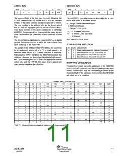
S
1
0
0
1
0
A
A
W
A
SD
C
C
C
PD PD X
0
X
A
1
0
2
1
0
1
Command Byte
Write-Addressing Byte
ADC Power-Down Mode
(depending on power-down selection bits)
ADC Converting Mode
Sr
1
0
0
1
0
A
A
R
A
D
D
D
D
D
D
D
D
0
N
P
1
0
7
6
5
4
3
2
1
See Note (1)
Read-Addressing Byte
1 x (8 Bits + not-ack)
A = acknowledge (SDA LOW)
N = not acknowledge (SDA HIGH)
S = START Condition
P = STOP Condition
Sr = repeated START condition
W = '0' (WRITE)
R = '1' (READ)
From Master to Slave
From Slave to Master
NOTE: (1) To secure bus operation and loop back to the stage of write-addressing for next conversion, use repeated START.
FIGURE 3. Typical Read Sequence in F/S Mode.
ADS7830
SBAS302
12
www.ti.com

 BB [ BURR-BROWN CORPORATION ]