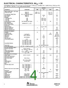
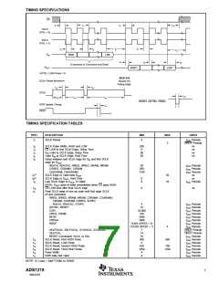
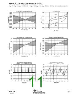
TIMING SPECIFICATIONS
CS
t3
t1
t2
t10
SCLK
(POL = 0)
SCLK
(POL = 1)
t2
t4
t5
t6
t11
DIN
MSB
LSB
t7
t8
t9
(Command or Command and Data)
MSB(1)
LSB(1)
DOUT
NOTE: (1) Bit Order = 0.
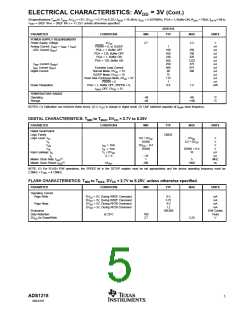
ADS1218
SCLK Reset Waveform
t13
Resets On
Falling Edge
t13
SCLK
t16
t12
t14
t15
RESET, DSYNC, PDWN
DDR Update Timing
DRDY
t17
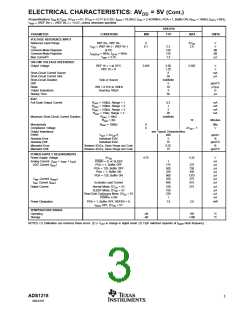
TIMING SPECIFICATION TABLES
SPEC
DESCRIPTION
MIN
MAX
UNITS
t1
SCLK Period
4
tOSC Periods
3
DRDY Periods
t2
t3
t4
t5
t6
SCLK Pulse Width, HIGH and LOW
CS LOW to first SCLK Edge; Setup Time
DIN Valid to SCLK Edge; Setup Time
Valid DIN to SCLK Edge; Hold Time
200
0
50
50
ns
ns
ns
ns
Delay between last SCLK edge for DIN and first SCLK
edge for DOUT
:
RDATA, RDATAC, RREG, WREG, RRAM, WRAM
CSREG, CSRAMX, CSRAM
CHKARAM, CHKARAMX
50
200
1100
tOSC Periods
tOSC Periods
tOSC Periods
ns
(1)
t7
t8
SCLK Edge to Valid New DOUT
SCLK Edge to DOUT, Hold Time
Last SCLK Edge to DOUT Tri-State
50
10
(1)
0
6
ns
t9
tOSC Periods
NOTE: DOUT goes tri-state immediately when CS goes HIGH.
t10
t11
CS LOW time after final SCLK edge
Final SCLK edge of one op code until first edge SCLK
0
ns
of next command:
RREG, WREG, RRAM, WRAM, CSRAMX, CSARAMX,
CSRAM, CSARAM, CSREG, SLEEP,
RDATA, RDATAC, STOPC
DSYNC, RESET
CSFL
CREG, CRAM
RF2R
CREGA
4
16
33,000
220
1090
1600
tOSC Periods
tOSC Periods
tOSC Periods
tOSC Periods
tOSC Periods
tOSC Periods
tOSC Periods
tOSC Periods
DRDY Periods
DRDY Periods
tOSC Periods
tOSC Periods
tOSC Periods
tOSC Periods
tOSC Periods
tOSC Periods
tOSC Periods
WR2F
76,850 (SPEED = 0)
101,050 (SPEED = 1)
4
SELFGCAL, SELFOCAL, SYSOCAL, SYSGCAL
SELFCAL
RESET (Command, SCLK, or Pin)
SCLK Reset, First HIGH Pulse
SCLK Reset, LOW Pulse
SCLK Reset, Second HIGH Pulse
SCLK Reset, Third HIGH Pulse
Pulse Width
7
14
16
300
5
550
1050
4
t12
t13
t14
t15
t16
t17
500
750
1250
DOR Data Not Valid
4
NOTE: (1) Load = 20pF 10kΩ to DGND.
ADS1218
7
SBAS187

 BB [ BURR-BROWN CORPORATION ]