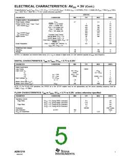
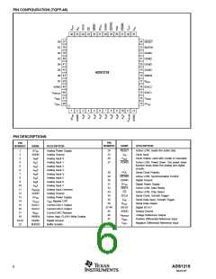
PIN CONFIGURATION (TQFP-48)
36 35 34 33 32 31 30 29 28 27 26 25
D0 37
D1 38
24 RESET
23 BUFEN
22 DGND
21 DGND
20 DGND
19 DGND
18 WREN
17 RDAC
D2 39
D3 40
D4 41
D5 42
ADS1218
D6 43
D7 44
AGND 45
VREFOUT 46
VREF+ 47
VREF– 48
16 IDAC2
15 IDAC1
14 VRCAP
13 AVDD
1
2
3
4
5
6
7
8
9
10 11 12
PIN DESCRIPTIONS
PIN
PIN
NUMBER
NAME
DESCRIPTION
NUMBER
NAME
DESCRIPTION
24
25
26
27
RESET
XIN
Active LOW, resets the entire chip.
Clock Input
1
2
AVDD
Analog Power Supply
Analog Ground
AGND
XOUT
Clock Output, used with crystal or resonator.
3
A
IN0
Analog Input 0
PDWN
Active LOW. Power Down. The power down
function shuts down the analog and digital
circuits.
4
AIN
1
Analog Input 1
5
A
A
IN2
IN3
Analog Input 2
6
Analog Input 3
28
29
POL
DSYNC
DGND
DVDD
DRDY
CS
Serial Clock Polarity
7
AIN
4
Analog Input 4
Active LOW, Synchronization Control
Digital Ground
8
A
A
IN5
IN6
Analog Input 5
30
9
Analog Input 6
31
Digital Power Supply
10
11
12
13
14
15
16
17
18
19-22
23
AIN
7
Analog Input 7
32
Active LOW, Data Ready
Active LOW, Chip Select
Serial Clock, Schmitt Trigger
Serial Data Input, Schmitt Trigger
Serial Data Output
AINCOM
AGND
AVDD
Analog Input Common
Analog Ground
33
34
SCLK
DIN
Analog Power Supply
VREF Bypass CAP
Current DAC1 Output
Current DAC2 Output
Current DAC Resistor
35
VRCAP
IDAC1
IDAC2
RDAC
36
DOUT
37-44
45
D0-D7
AGND
VREFOUT
VREF+
VREF–
Digital I/O 0-7
Analog Ground
46
Voltage Reference Output
Positive Differential Reference Input
Negative Differential Reference Input
WREN
DGND
BUFEN
Active High, FLASH Write Enable
Digital Ground
47
48
Buffer Enable
ADS1218
6
SBAS187

 BB [ BURR-BROWN CORPORATION ]