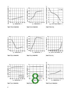
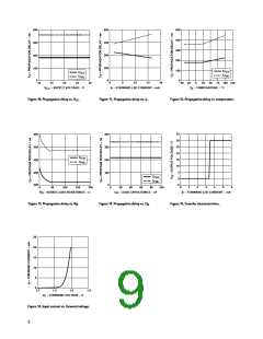
CMR with the LED On (CMR )
supplied by the LED, and it is
not recommended for
applications requiring ultra high
condition is equal to the
maximum value of the
H
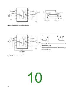
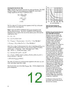
A high CMR LED drive circuit
must keep the LED on during
common mode transients. This is
achieved by overdriving the LED
current beyond the input
threshold so that it is not pulled
below the threshold during a
transient. A minimum LED
current of 8 mA provides
propagation delay difference
specification, PDD max, which is
specified to be 500 ns over the
operating temperature range of
-40° to 100°C.
CMR performance. The
1
alternative drive circuit which
like the recommended
application circuit (Figure 19),
does achieve ultra high CMR
performance by shunting the
LED in the off state.
Delaying the LED signal by the
maximum propagation delay
difference ensures that the
adequate margin over the
maximum I
achieve 10 kV/µs CMR.
of 5 mA to
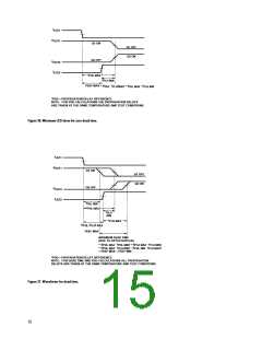
IPM Dead Time and Propagation
Delay Specifications
minimum dead time is zero, but it
does not tell a designer what the
maximum dead time will be. The
maximum dead time is equivalent
to the difference between the
maximum and minimum
FLH
The HCPL-3140/HCPL-0314
includes a Propagation Delay
Difference (PDD) specification
intended to help designers
minimize “dead time” in their
power inverter designs. Dead
time is the time high and low
side power transistors are off.
Any overlap in Ql and Q2
conduction will result in large
currents flowing through the
power devices from the high-
voltage to the low-voltage motor
rails. To minimize dead time in a
given design, the turn on of
LED2 should be delayed (relative
to the turn off of LED1) so that
under worst-case conditions,
transistor Q1 has just turned off
when transistor Q2 turns on, as
shown in Figure 26. The amount
of delay necessary to achieve this
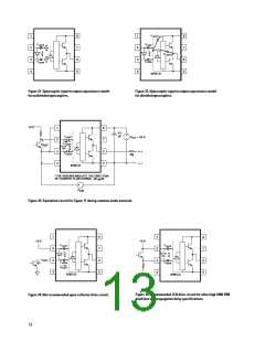
CMR with the LED Off (CMR )
L
A high CMR LED drive
circuit must keep the LED off
propagation delay difference
specification as shown in
(V ≤ V
) during common
F
F(OFF)
mode transients. For example,
during a -dV /dt transient in
Figure 23, the current flowing
Figure 27. The maximum dead
time for the HCPL-3140/HCPL-
0314 is 1 µs (= 0.5 µs - (-0.5 µs))
over the operating temperature
range of –40°C to 100°C.
CM
through C
also flows
LEDP
through the R
logic gate. As long as the low
state voltage developed across
the logic gate is less than V
the LED will remain off and no
common mode failure will occur.
and V
of the
SAT
SAT
Note that the propagation delays
used to calculate PDD and dead
time are taken at equal
temperatures and test conditions
since the optocouplers under
consideration are typically
mounted in close proximity to
each other and are switching
identical IGBTs.
F(OFF)
The open collector drive circuit,
shown in Figure 24, can not keep
the LED off during a + dV /dt
transient, since all the current
flowing through C
CM
must be
LEDN
14

 AVAGO [ AVAGO TECHNOLOGIES LIMITED ]