4.0
3.5
3.0
2.5
2.0
1.5
1.0
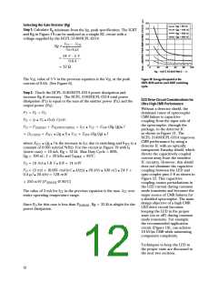
Selecting the Gate Resistor (Rg)
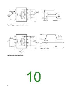
Step 1: Calculate R minimum from the I peak specification. The IGBT
and Rg in Figure 19 can be analyzed as a simple RC circuit with a
voltage supplied by the HCPL-3140/HCPL-0314.
Qg = 50 nC
Qg = 100 nC
Qg = 200 nC
Qg = 400 nC
g
OL
V
– V
CC
OL
Rg ≥
I
OLPEAK
24 V – 5 V
0.6A
=
0.5
0
= 32 Ω
0
20
40
60
80
100
Rg – GATE RESISTANCE – Ω
The V value of 5 V in the previous equation is the V at the peak
current of 0.6A. (See Figure 6).
Figure 20. Energy dissipated in the
HCPL-0314 and for each IGBT switching
cycle.
OL
OL
Step 2: Check the HCPL-3140/HCPL-0314 power dissipation and
increase Rg if necessary. The HCPL-3140/HCPL-0314 total power
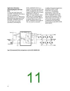
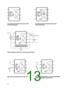
LED Drive Circuit Considerations for
Ultra High CMR Performance
Without a detector shield, the
dominant cause of optocoupler
CMR failure is capacitive
coupling from the input side of
the optocoupler, through the
package, to the detector IC
dissipation (P ) is equal to the sum of the emitter power (P ) and the
T
E
output power (P ).
O
P = P + P
T
E
O
E
O
P
P
= I
V
Duty Cycle
+ P
•
•
F
F
= P
= I
V
CC
+ E
(Rg,Qg) f
•
SW
•
O(BIAS)
O(SWITCHING)
CC
as shown in Figure 21. The
= (I
+ K
Qg f)
V
CC
+ E
(Rg,Qg)
f
•
•
•
•
CCBIAS
ICC
SW
HCPL-3140/HCPL-0314 improves
CMR performance by using a
detector IC with an optically
transparent Faraday shield, which
diverts the capacitively coupled
current away from the sensitive
IC circuitry. However, this shield
does not eliminate the capacitive
coupling between the LED and
opto-coupler pins 5-8 as shown in
Figure 22. This capacitive
coupling causes perturbations in
the LED current during common
mode transients and becomes the
major source of CMR failures for
a shielded optocoupler. The main
design objective of a high CMR
LED drive circuit becomes
where K
Qg f is the increase in I due to switching and K
is a
•
•
CC
ICC
ICC
constant of 0.001 mA/(nC*kHz). For the circuit in Figure 19 with I
(worst case) = 10 mA, Rg = 32 Ω, Max Duty Cycle = 80%,
Qg = 100 nC, f = 20 kHz and T
F
= 85°C:
AMAX
P
P
= 10 mA 1.8 V 0.8 = 14 mW
• •
E
= (3 mA + (0.001 mA/(nC kHz)) 20 kHz 100 nC) 24 V +
•
•
•
•
O
0.4 µJ 20 kHz = 128 mW
•
< 250 mW (P
@ 85°C)
O(MAX)
The value of 3 mA for I in the previous equation is the max. I over
entire operating temperature range.
CC
CC
Since P for this case is less than P
, Rg = 32 Ω is alright for the
O(MAX)
O
power dissipation.
keeping the LED in the proper
state (on or off) during common
mode transients. For example,
the recommended application
circuit (Figure 19), can achieve
10 kV/µs CMR while minimizing
component complexity.
Techniques to keep the LED in
the proper state are discussed in
the next two sections.
12

 AVAGO [ AVAGO TECHNOLOGIES LIMITED ]