C
1
2
3
4
8
7
6
5
1
2
3
4
8
7
6
5
LEDO1
C
C
C
C
LEDP
LEDP
C
LEDO2
LEDN
LEDN
SHIELD
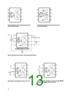
Figure 21. Optocoupler input to output capacitance model
forunshieldedoptocouplers.
Figure 22. Optocoupler input to output capacitance model
forshieldedoptocouplers.
+5 V
1
2
3
4
8
7
6
5
0.1
µF
+
–
C
I
LEDP
V
= 18 V
CC
+
LEDP
V
SAT
–
• • •
• • •
C
LEDN
Rg
SHIELD
* THE ARROWS INDICATE THE DIRECTION
OF CURRENT FLOW DURING –dV /dt.
CM
+
–
V
CM
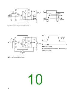
Figure 23. Equivalent circuit for Figure 17 during common mode transient.
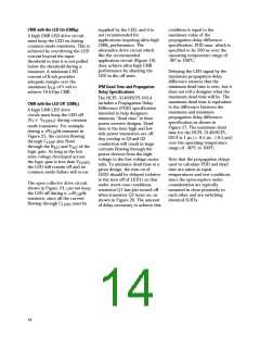
1
2
3
4
8
7
6
5
1
2
3
4
8
7
6
5
+5 V
+5 V
C
C
C
LEDP
LEDP
C
I
LEDN
LEDN
Q1
LEDN
SHIELD
SHIELD
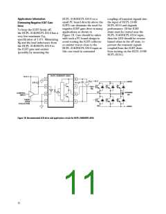
Figure 25. Recommended LED drive circuit for ultra-high CMR IPM
dead time and propagation delay specifications.
Figure 24. Not recommended open collector drive circuit.
13

 AVAGO [ AVAGO TECHNOLOGIES LIMITED ]