VRAM
SMJ44C251B
MT42C4256
Austin Semiconductor, Inc.
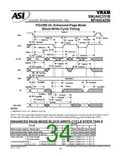
FIGURE 24: Enhanced-Page-Mode
Block-Write-Cycle Timing
NOTES:
1. Referenced to CAS\ or W\, whichever occurs last
NOTE D: TRG\ must remain high throughout the entire page-mode operation to assure page-mode cycle time if the late write feature is used. If
the early-write-cycle timing is used, the state of TRG\ is a don’t care after the minimum period th(TRG) from the falling edge of RAS\.
ENHANCED-PAGE-MODE BLOCK-WRITE-CYCLE STATE TABLE
STATE
CYCLE
1
L
H
L
2
L
L
3
4
Write-mask load/use, Block write
Use previous write mask, Block write
Write mask disable, Block write to all I/Os
Write mask data 0: I/O write disable
1: I/O write enable
Write Mask Column Mask
Don't Care Column Mask
Don't Care Column Mask
H
DQ0 — column 0 (addressA1 = 0,A0 = 0)
DQ1 — column 1 (addressA1 = 0,A0 = 1)
DQ2 — column 2 (addressA1 = 1,A0 = 0)
Column mask data DQn =
(n = 0, 1, 2, 3)
0 column write disable
1 column write enable
DQ3 — column 3 (addressA1 = 1,A0 = 1)
Austin Semiconductor, Inc. reserves the right to change products or specifications without notice.
SMJ44C251B/MT42C4256
Rev. 0.1 12/03
34

 AUSTIN [ AUSTIN SEMICONDUCTOR ]