AUSTIN SEMICONDUCTOR, INC.
FLASH
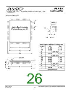
AS8FLC2M32
Austin Semiconductor, Inc.
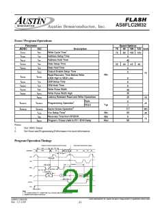
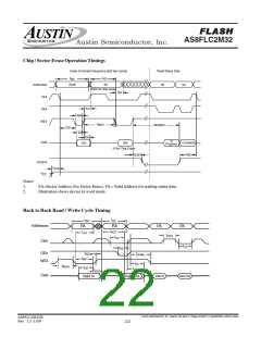
Chip / Sector Erase Operation Timings
Erase Command Sequence (last two cycles)
Read Status Data
t
t
AS
SA
WC
Addresses
CE#
2AAh
VA
VA
555h for chip erase
t
AH
t
CH
OE#
t
WP
WE#
t
t
WPH
WHWH2
t
CS
t
DS
t
DH
In
Data
Complete
30h
55h
Progress
10 for Chip Erase
t
t
RB
BUSY
RY/BY#
t
VCS
V
CC
Notes:
1.
2.
SA=Sector Address (for Sector Erase), VA= Valid Address for reading status data.
Illustration shows device in word mode.
Back to Back Read / Write Cycle Timing
t
t
RC
WC
Addresses
PA
RA
PA
PA
t
t
ACC
t
AH
t
CPH
CE
CE#
t
CP
t
OE
t
OE#
WE#
t
SR/W
GHWL
t
WP
t
t
DF
t
WDH
DS
t
OH
t
DH
Data
Valid In
Valid Out
Valid In
Valid Out
Austin Semiconductor, Inc. reserves the right to change products or specifications without notice.
AS8FLC2M32B
Rev. 1.2 5/09
22

 AUSTIN [ AUSTIN SEMICONDUCTOR ]